SmartFusion2 SoC FPGA - Cache Controller Configuration - Libero SoC v11.7
4 Revision 10
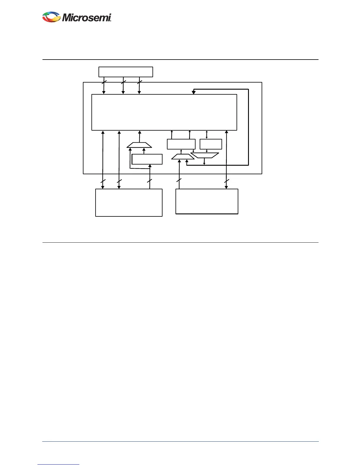
Figure 2 shows the block diagram of the SmartFusion2 cache controller. Refer to the
UG0331: SmartFusion2 Microcontroller Subsystem User Guide for more information on cache controller.
Cacheable Memory Regions
The following sections explain memory mapping of eNVM and LPDDR address space to cacheable
memory regions. The code space of the ARM
®
Cortex
®
-M3 processor ranges from 0x00000000 to
0x1FFFFFFF (0.5 GB). The address space of eNVM or LPDDR can be mapped to code space of the
Cortex-M3 processor to make the memory region cacheable. Design examples are provided in
"Appendix: Design and Programming Files" on page 16.
Remapping eNVM as Cacheable Region
The address range of eNVM_0 is from 0×60000000 to 0×6003FFFF and the address range of eNVM_1
is from 0×60040000 to 0×6007FFFF. By default, the full eNVM memory from 0×60000000 to
0×6007FFFF is mapped as a cacheable region. The eNVM base address 0×60000000 is remapped to
Corte×-M3 processor address space 0×00000000. You can remap any offset of eNVM address to the
Corte×-M3 processor address space 0×00000000 by using the ENVM_CR, ENVM_REMAPSIZE, and
ENVM_REMAP_BASR_CR system registers.
Figure 2 • SmartFusion2 Device Cache Controller Block Diagram
&RUWH[03URFHVVRU
$+%%XV0DWUL[
066''5%ULGJH
00
'
00
,
00
6
00
&
'5:
06
65:
06
,&5
06
' 5
06
,5
06
65:
06
':
65:
06
&DFKH0DWUL[[
3LSHOLQH3UHIHWFK
%XIIHU
&DFKH(QJLQH
$+%WR0 (0
'(&
'5: 6\VWHP&RQWU ROOHU
%XV 5:
,&5 ,'&5 ':6*5:
7RF DFKHP HPRU\
000LUURUHG0DVWHU 060LUURUHG6ODYH'6* 'DWD6\VWHPDQG6\VWHPFRQWUROOHU%XV
,'& ,FRGHDQG'&RGH&DFKHDEOH ,,QVWUXFWLRQ 66\VWHP55HDG''DWD: ZULWH