© 2009 MIMAKI ENGINEERING CO.,LTD.
1.1.2 P.1
1
2
3
4
5
6
7
8
R.1.1
Maintenance Manual > Operating Principle > Basic Operation > Sub Switch Power ON
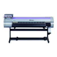
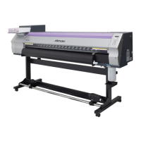
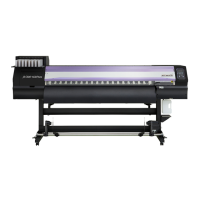
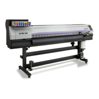
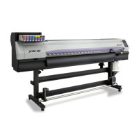
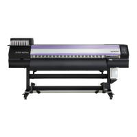
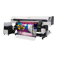
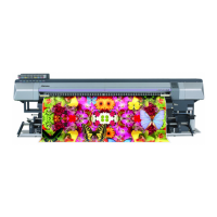
Model CJV30/TPC Issued 2008.08.04 Revised 2008.09.17 F/W ver. 1.20 Remark
1.1
1.1.2 Sub Switch Power ON
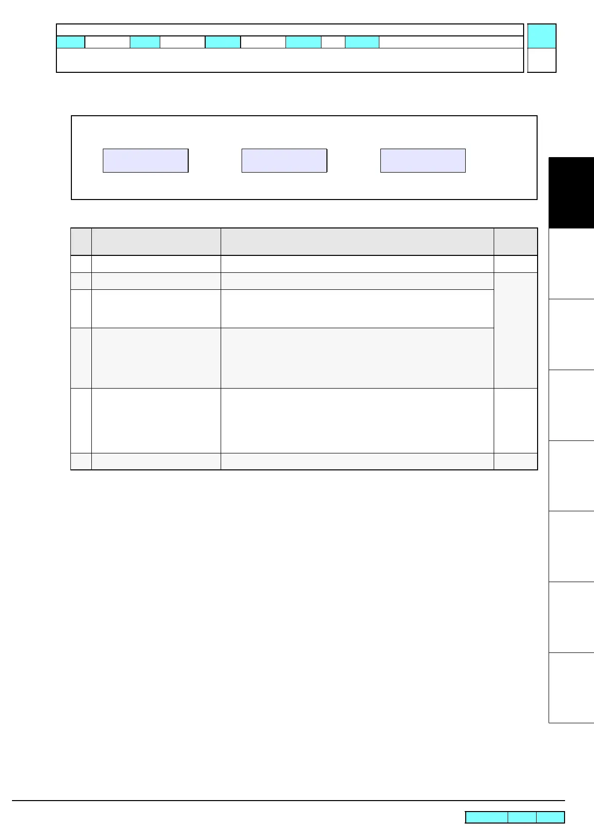
Indication on LCD
Processing sequence
Step Processing Description
Indication
on LCD
1 Initial setting of CPU and H/W
2 Display at sub switch power ON 1. [PLEASE WAIT] is displayed.
3 Voltage check 1. Check the power supply voltage on the main PCB assy.
• In the malfunction, [ERROR03 POWER **V] is displayed and the
system goes down.
4 FPGA setting 1. Execute the configuration of PDC and HDC.
• In the malfunction, [ERROR09 FPGA ERROR] is displayed and
the system goes down.
• When the fuse F13 of the main PCB assy is blown, the system shuts
down, displaying [EEROR25 47V HEAD VOLTAGE].
5 Version information display 1. Machine model name and main body firmware version are displayed.
2. “Revision” and “PDC/HDC version” are also displayed during the
service mode.
3. Special key function is workable during the version information is
being displayed. (Except firmware update)
6 Initial operation of the printer 1. Refer to "1.1.3 Initial Machine Operation" .
Display at sub switch power ON
PLEASE WAIT
Version information display
CJV30-100 V1.00
Version information display
(during the service mode)
CJV30-100 V1.00.0
P.1.0.H.1.0
P: PDC, H: HDC
 Loading...