Signal Description
5-12 MC68030 USER’S MANUAL MOTOROLA
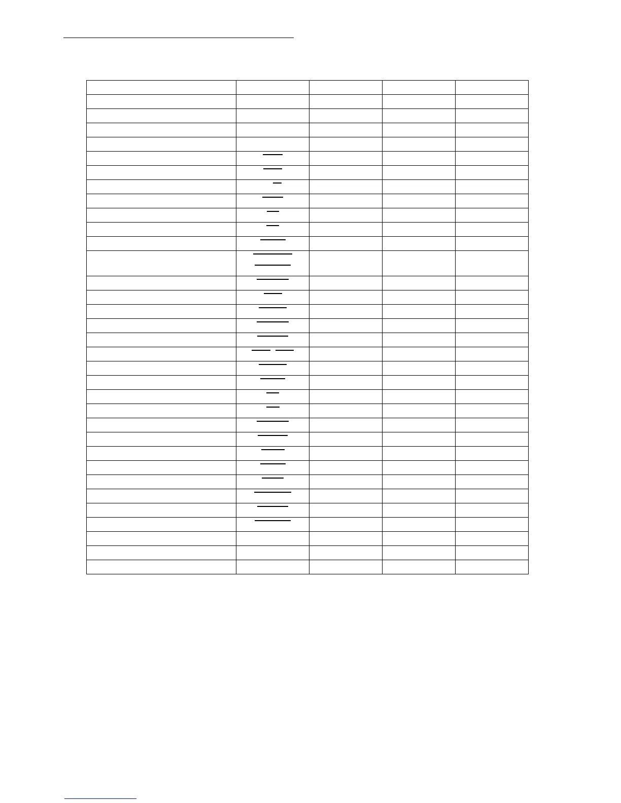
Table 5-2. Signal Summary
Signal Function Signal Name Input/Output Active State Three-State
Function Codes
FC0–FC2 Output High Yes
Address Bus A0–A31 Output High Yes
Data Bus D0–D31 Input/Output High Yes
Transfer Size SIZ0/SIZ1 Output High Yes
Operand Cycle Start OCS
Output Low No
External Cycle Start ECS
Output Low No
Read/Write R/W
Output High/Low Yes
Read-Modify-Write Cycle RMC
Output Low Yes
Address Strobe AS
Output Low Yes
Data Strobe DS
Output Low Yes
Data Buffer Enable DBEN
Output Low Yes
Data Transfer and Size
Acknowledge
DSACK0/
DSACK1
Input Low —
Synchronous Termination STERM
Input Low —
Cache Inhibit In CIIN
Input Low —
Cache Inhibit Out CIOUT
Output Low Yes
Cache Burst Request CBREQ
Output Low Yes
Cache Burst Acknowledge CBACK
Input Low —
Interrupt Priority Level IPL0
–IPL2 Input Low —
Interrupt Pending IPEND
Output Low No
Autovector AVEC
Input Low —
Bus Request BR
Input Low —
Bus Grant BG
Output Low No
Bus Grant Acknowledge BGACK
Input Low —
Reset RESET
Input/Output Low No
Halt HALT
Input Low —
Bus Error BERR
Input Low —
Cache Disable CDIS
Input Low —
MMU Disable MMUDIS
Input Low —
Pipeline Refill REFILL
Output Low No
Microsequencer Status STATUS
Output Low No
Clock CLK Input — —
Power Supply VCC Input — —
Ground GND Input — —

 Loading...
