Bus Operation
7-105 MC68030 USER’S MANUAL MOTOROLA
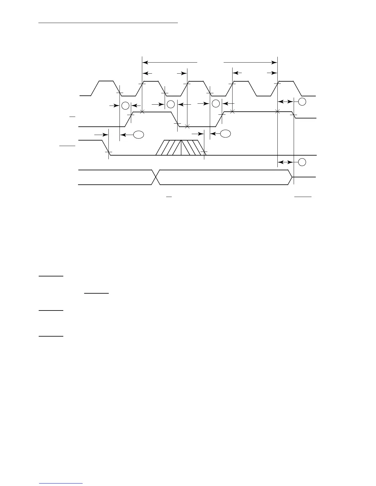
A timing diagram of the bus arbitration sequence during a processor bus cycle is shown in
Figure 7-60. The bus arbitration sequence while the bus is inactive (i.e., executing internal
operations such as a multiply instruction) is shown in Figure 7-63.
7.8 RESET OPERATION
RESET is a bidirectional signal with which an external device resets the system or the
processor resets external devices. When power is applied to the system, external circuitry
should assert RESET
for a minimum of 520 clocks after V
CC
is within tolerance. Figure 7-64
is a timing diagram of the powerup reset operation, showing the relationships between
RESET
, V
CC
, and bus signals. The clock signal is required to be stable by the time V
CC
reaches the minimum operating specification. During the reset period, the entire bus three-
states (except for non-three-statable signals, which are driven to their inactive state). Once
RESET
negates, all control signals are driven to their inactive state, the data bus is in read
mode, and the address bus is driven. After this, the first bus cycle for reset exception
processing begins.
Figure 7-62. Single-Wire Bus Arbitration Timing Diagram
NOTE: The alternate bus master must sample AS high on two consecutive rising edges of the clock (after BGACK is
recognized low) before taking the bus.
16
7
47A
12
TAKE BUS
SEE NOTE
DO NOT
TAKE BUS
9
12
47A
CLK
AS
BGACK
ADDRESS

 Loading...
