Operation 5-7
SG 2000 Installation and Operation Manual
4
Remove the eight screws that secure the SG2-RPM/C board to the chassis. Remove the
SG2-RPM/C board. To assist in removing the SG2-RPM/C board, the handle is cantilevered so
that pulling up on the handle extracts the board from the chassis.
5 Remove the 5-pin power connector that provided dc power to the SG2-RPM/C board.
6 Install the SG2-RPM/S board by reversing the above procedure. Do not re-install the 5-pin
power connector as the SG2-RPM/s does not require nor accept it.
Digital Return Path RF Configuration
If you are using a single DS-SG2-DRT/A transmitter, it must be installed in the optical transmitter A
position as illustrated in Figure 3-1. A JXP-5A (5 dB) pad is installed in the pad facility at the A
transmitter location. A JXP-15A (15 dB) pad must also be installed in the pad facility at the B
transmitter location to terminate the signal from the return-path-module combiner board
(SG2-RPM/C).
For single return applications, the SG2-LIDB distributes an individual RF signal from the RF chassis
to transmitter A. Installing an optional second transmitter (B) provides return redundancy as
illustrated in Figure 5-10. Installing a redundant B transmitter also requires that you change the pad
at that location to a JXP-5A.
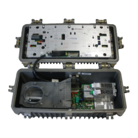
Figure 5-10
DS-SG2-DRT/A redundant return
SG2-RPM/C
SG2-RPLPF
Optional
transmitter
A
Transmitter
B
TP
TP
Bulkhead connector
for dc power
JXP
JXP
BASE
Status
monitor
JXP
In
ress
LID
TP
TP
H
L
LP filter
 Loading...