https://reference.digilentinc.com/reference/programmable-logic/nexys-a7/reference-manual 11/30
¹ Zynq-7000 SoC and 7 Series Devices Memory Interface Solutions from Xilinx
(http://www.xilinx.com/support/documentation/ip_documentation/mig_7series/v2_1/ug586_7Series_MIS.pdf)
² Spansion S25FL032P_00 Datasheet (https://www.spansion.com/Support/Datasheets/S25FL032P_00.pdf)
³ 7-Series FPGAs Configuration User Guide from Xilinx
(http://www.xilinx.com/support/documentation/user_guides/ug470_7Series_Config.pdf)
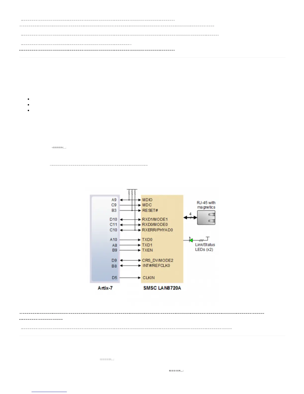
The Nexys A7 board includes an SMSC 10/100 Ethernet PHY (SMSC part number LAN8720A) paired with an RJ-45 Ethernet jack with
integrated magnetics. The SMSC PHY uses the RMII interface and supports 10/100 Mb/s. Figure 4.1 illustrates the pin connections
between the Artix-7 and the Ethernet PHY. At power-on reset, the PHY is set to the following defaults:
RMII mode interface
Auto-negotiation enabled, advertising all 10/100 mode capable
PHY address=00001
Two on-board LEDs (LD23 = LED2, LD24 = LED1) connected to the PHY provide link status and data activity feedback. See the PHY
datasheet for details.
EDK-based designs can access the PHY using either the axi_ethernetlite (AXI EthernetLite) IP core or the axi_ethernet (Tri Mode Ethernet
MAC) IP core. A mii_to_rmii core (Ethernet PHY MII to Reduced MII) needs to be inserted to convert the MAC interface from MII to
RMII. Also, a 50 MHz () clock needs to be generated for the mii_to_rmii core and the CLKIN pin of the external PHY. To account for
skew introduced by the mii_to_rmii core, generate each clock individually, with the external PHY clock having a 45 degree phase shift
relative to the mii_to_rmii Ref_Clk. An EDK demonstration project that properly uses the Ethernet PHY can be found on the Nexys A7
product page at www.digilentinc.com (http://www.digilentinc.com).
ISE designs can use the IP Core Generator wizard to create an Ethernet MAC controller IP core.
NOTE: Refer to the LAN8720A data sheet¹ for further information.
(https://reference.digilentinc.com/_detail/reference/programmable-logic/nexys-a7/n4g.png?id=reference%3Aprogrammable-logic%3Anexys-
a7%3Areference-manual) Figure 4.1 Pin Connections between the Artix-7 and the Ethernet PHY
¹ SMSC LAN8720A Datasheet from Microchip (http://ww1.microchip.com/downloads/en/DeviceDoc/8720a.pdf)
The Nexys A7 board includes a single 100 MHz () crystal oscillator connected to pin E3 (E3 is a MRCC input on bank 35). The input clock
can drive MMCMs or PLLs to generate clocks of various frequencies and with known phase relationships that may be needed throughout a
design. Some rules restrict which MMCMs and PLLs may be driven by the 100 MHz () input clock. For a full description of these rules and
of the capabilities of the Artix-7 clocking resources, refer to the “7 Series FPGAs Clocking Resources User Guide” available from Xilinx.
4 Ethernet PHY
5 Oscillators/Clocks