https://reference.digilentinc.com/reference/programmable-logic/nexys-a7/reference-manual 22/30
(https://reference.digilentinc.com/_detail/reference/programmable-logic/nexys-a7/n4u.png?id=reference%3Aprogrammable-logic%3Anexys-
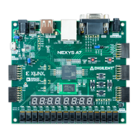
a7%3Areference-manual) Figure 9.1.3 Four Digit Scanning Display Controller Timing Diagram
The Nexys A7 board contains two tri-color LEDs. Each tri-color LED () has three input signals that drive the cathodes of three smaller
internal LEDs: one red, one blue, and one green. Driving the signal corresponding to one of these colors high will illuminate the internal
LED (). The input signals are driven by the FPGA through a transistor, which inverts the signals. Therefore, to light up the tri-color LED (),
the corresponding signals need to be driven high. The tri-color LED () will emit a color dependent on the combination of internal LEDs
that are currently being illuminated. For example, if the red and blue signals are driven high, and green is driven low, the tri-color LED ()
will emit a purple color.
Note: Digilent strongly recommends the use of pulse-width modulation (PWM) when driving the tri-color LEDs (for information on PWM,
see section 15.1 Pulse Density Modulation (PDM)). Driving any of the inputs to a steady logic ‘1’ will result in the LED () being illuminated
at an uncomfortably bright level. You can avoid this by ensuring that none of the tri-color signals are driven with more than a 50% duty
cycle. Using PWM also greatly expands the potential color palette of the tri-color led. Individually adjusting the duty cycle of each color
between 50% and 0% causes the different colors to be illuminated at different intensities, allowing virtually any color to be displayed.
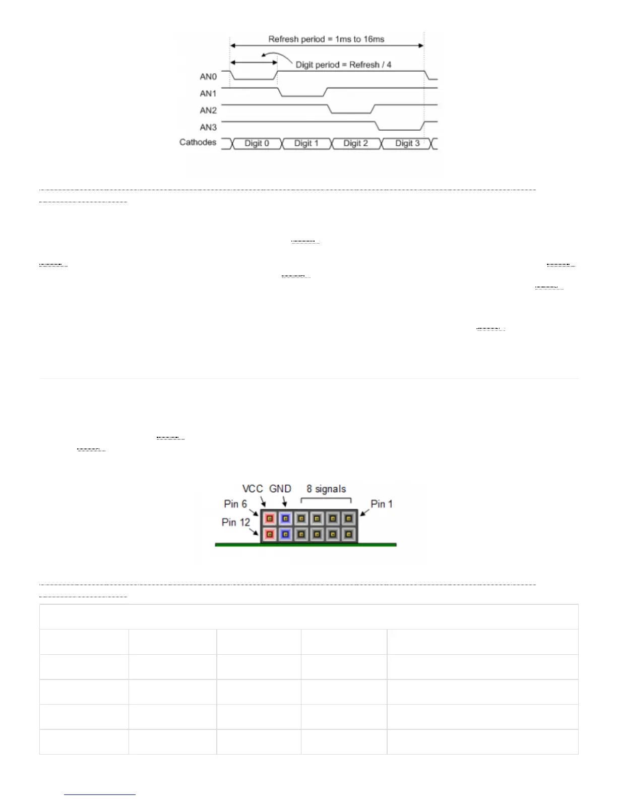
The Pmod ports are arranged in a 2×6 right-angle, and are 100-mil female connectors that mate with standard 2×6 pin headers. Each 12-pin
Pmod port provides two 3.3V VCC () signals (pins 6 and 12), two Ground signals (pins 5 and 11), and eight logic signals, as shown in Figure
10.1. The VCC () and Ground pins can deliver up to 1A of current. Pmod data signals are not matched pairs, and they are routed using best-
available tracks without impedance control or delay matching. Pin assignments for the Pmod I/O connected to the FPGA are shown in
Table 5.
(https://reference.digilentinc.com/_detail/reference/programmable-logic/nexys-a7/n4v.png?id=reference%3Aprogrammable-logic%3Anexys-
a7%3Areference-manual) Figure 10.1 Pmod Connectors; Front View, as Loaded on PCB
Table 10.1. Nexys A7 Pmod pin assignments.
Pmod JA Pmod JB Pmod JC Pmod JD Pmod XDAC
JA1: C17 JB1: D14 JC1: K1 JD1: H4 JXADC1: A13 (AD3P)
JA2: D18 JB2: F16 JC2: F6 JD2: H1 JXADC2: A15 (AD10P)
JA3: E18 JB3: G16 JC3: J2 JD3: G1 JXADC3: B16 (AD2P)
JA4: G17 JB4: H14 JC4: G6 JD4: G3 JXADC4: B18 (AD11P)
9.2 Tri-Color LED
10 Pmod Ports