https://reference.digilentinc.com/reference/programmable-logic/nexys-a7/reference-manual 8/30
After power-on, the Artix-7 FPGA must be configured (or programmed) before it can perform any functions. You can configure the FPGA
in one of four ways:
1. A PC can use the Digilent USB-JTAG circuitry (portJ6, labeled “PROG”) to program the FPGA any time the power is on.
2. A file stored in the nonvolatile serial (SPI) flash device can be transferred to the FPGA using the SPI port.
3. A programming file can be transferred to the FPGA from a micro SD card.
4. A programming file can be transferred from a USB memory stick attached to the USB HID port.
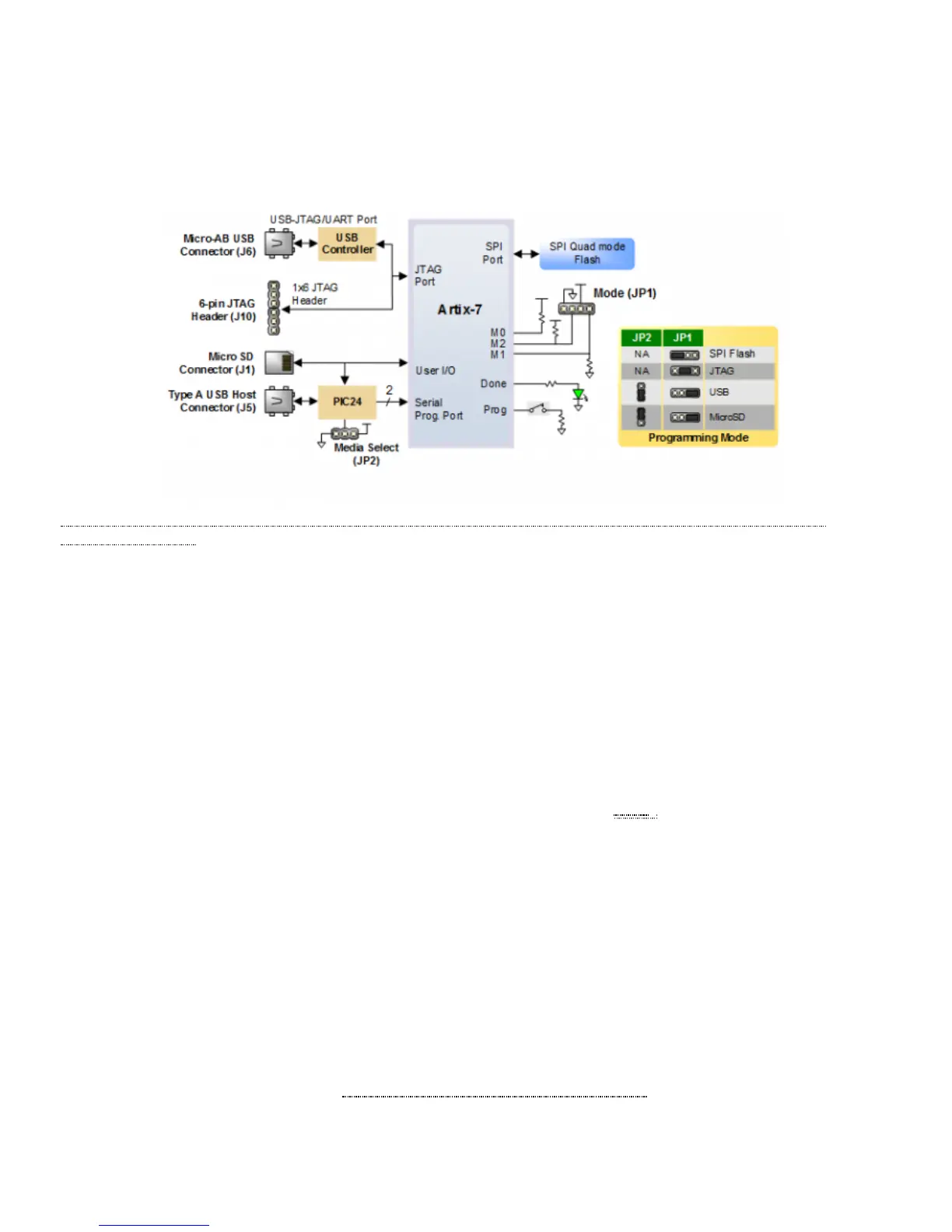
(https://reference.digilentinc.com/_detail/reference/programmable-logic/nexys-a7/n4e.png?id=reference%3Aprogrammable-logic%3Anexys-
a7%3Areference-manual) Figure 2.1 Nexys A7 DDR Configuration Options
Figure 2.1 shows the different options available for configuring the FPGA. An on-board “mode” jumper (JP1) and a media selection jumper
(JP2) select between the programming modes.
The FPGA configuration data is stored in files called bitstreams that have the .bit file extension. The ISE or Vivado software from Xilinx
can create bitstreams from VHDL, Verilog®, or schematic-based source files (in the ISE toolset, EDK is used for MicroBlaze™ embedded
processor-based designs).
Bitstreams are stored in SRAM-based memory cells within the FPGA. This data defines the FPGA’s logic functions and circuit connections,
and it remains valid until it is erased by removing board power, by pressing the reset button attached to the PROG input, or by writing a
new configuration file using the JTAG port.
An Artix-7 100T bitstream is typically 30,606,304 bits and can take a long time to transfer. The time it takes to program the Nexys A7 can
be decreased by compressing the bitstream before programming, and then allowing the FPGA to decompress the bitstream itself during
configuration. Depending on design complexity, compression ratios of 10x can be achieved. Bitstream compression can be enabled within
the Xilinx tools (ISE or Vivado) to occur during generation. For instructions on how to do this, consult the Xilinx documentation for the
toolset being used. After being successfully programmed, the FPGA will cause the “DONE” LED () to illuminate. Pressing the “PROG”
button at any time will reset the configuration memory in the FPGA. After being reset, the FPGA will immediately attempt to reprogram
itself from whatever method has been selected by the programming mode jumpers.
The following sections provide greater detail about programming the Nexys A7 using the different methods available.
The Xilinx tools typically communicate with FPGAs using the Test Access Port and Boundary-Scan Architecture, commonly referred to as
JTAG. During JTAG programming, a .bit file is transferred from the PC to the FPGA using the onboard Digilent USB-JTAG circuitry (port
J6) or an external JTAG programmer, such as the Digilent JTAG-HS2, attached to port J10. You can perform JTAG programming any time
after the Nexys A7 has been powered on, regardless of what the mode jumper (JP1) is set to. If the FPGA is already configured, then the
existing configuration is overwritten with the bitstream being transmitted over JTAG. Setting the mode jumper to the JTAG setting (seen in
Figure 3) is useful to prevent the FPGA from being configured from any other bitstream source until a JTAG programming occurs.
Programming the Nexys A7 with an uncompressed bitstream using the on-board USB-JTAG circuitry usually takes around five seconds.
JTAG programming can be done using the hardware server in Vivado or the iMPACT tool included with ISE and the Lab Tools version of
Vivado. The demonstration project available at www.digilentinc.com (http://www.digilentinc.com) gives an in-depth tutorial on how to
program your board.
2 FPGA Configuration
2.1 JTAG Configuration
2.2 Quad-SPI Configuration
 Loading...