EasyManua.ls Logo

Nexys A7 User Manual

Nexys A7
30 pages
To Next Page IconTo Next Page
Page #1 background imageLoading...
Page #1 background image
12/25/2018 Nexys A7 Reference Manual [Reference.Digilentinc]
https://reference.digilentinc.com/reference/programmable-logic/nexys-a7/reference-manual 1/30
The Nexys A7 board is a complete, ready-to-use digital circuit development platform based on the latest Artix-7™ Field Programmable
Gate Array (FPGA) from Xilinx®. With its large, high-capacity FPGA, generous external memories, and collection of USB, Ethernet, and
other ports, the Nexys A7 can host designs ranging from introductory combinational circuits to powerful embedded processors. Several
built-in peripherals, including an accelerometer, temperature sensor, MEMs digital microphone, a speaker amplifier, and several I/O devices
allow the Nexys A7 to be used for a wide range of designs without needing any other components.
(https://reference.digilentinc.com/_media/reference/programmable-logic/nexys-a7/nexys-a7-obl-600.png)
Nexys A7 Reference Manual
Question and Answer IconNeed help?

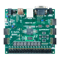
Do you have a question about the Nexys A7 and is the answer not in the manual?

Nexys A7 Specifications

General IconGeneral
FPGA FamilyArtix-7
FPGA Part NumberXC7A100T-1CSG324C
Logic Cells101, 440
CLB Flip-Flops126, 800
Block RAM4, 860 Kbits
DSP Slices240
On-Chip ADCYes
System Clock100 MHz
USB-UART BridgeYes
USB HostYes
USB HIDYes
MicroSD Card ConnectorYes
Pmod Connectors4
XADC HeaderYes
User LEDs16
User Pushbuttons5
User Switches16
7-Segment Displays8
HDMI SinkNo
HDMI SourceNo
Ethernet Speed10/100 Mbps
Expansion ConnectorsPmod, XADC
Power SupplyUSB
RAM128 MB
Onboard Memory16 MB

Summary

Key Features Overview

Artix-7 FPGA

Overview of the FPGA's programmable logic slices, LUTs, and flip-flops.

Functional Description and Power

Power Supplies

Describes how the Nexys A7 board is powered and its power circuitry.

Protection Circuitry

Details on overcurrent and overvoltage protection mechanisms on the board.

FPGA Configuration Methods

JTAG Configuration

How to program the FPGA using the JTAG interface via USB.

Quad-SPI Configuration

Programming the FPGA using the onboard Quad-SPI flash memory.

Onboard Memory

DDR2 Memory

Details on the 128MiB DDR2 SDRAM, its interface, and controller options.

Quad-SPI Flash Storage

Information on the non-volatile serial flash memory for configuration storage.

USB-UART Serial Communication

FT2232HQ Functionality

Details on the USB-UART bridge for serial communication with the FPGA.

VGA Video Output

Pmod Expansion Ports

MicroSD Card Interface

Hardware Self-Test

Demo Configuration Overview

How the onboard demo configuration verifies hardware components.