https://reference.digilentinc.com/reference/programmable-logic/nexys-a7/reference-manual 10/30
Table 3.1.1 DDR2 settings for the Nexys A7.
Setting Value
Memory type DDR2 SDRAM
Max. clock period 3000ps (667Mbps data rate)
Recommended clock period (for easy clock generation) 3077ps (650Mbps data rate)
Memory part MT47H64M16HR-25E
Data width 16
Data mask Enabled
Chip Select pin Enabled
Rtt (nominal) – On-die termination 50ohms
Internal Vref Enabled
Internal termination impedance 50ohms
Although the FPGA, memory IC, and the board itself are capable of the maximum data rate of 667Mbps, the limitations in the clock
generation primitives restrict the clock frequencies that can be generated from the 100 MHz () system clock. Thus, for simplicity, the next
highest data rate of 650Mbps is recommended.
The MIG Wizard will require the fixed pin-out of the memory signals to be entered and validated before generating the IP core. For your
convenience, an importable UCF file is provided on the Digilent website to speed up the process.
For more details on the Xilinx memory interface solutions, refer to the 7 Series FPGAs Memory Interface Solutions User Guide (ug586)¹.
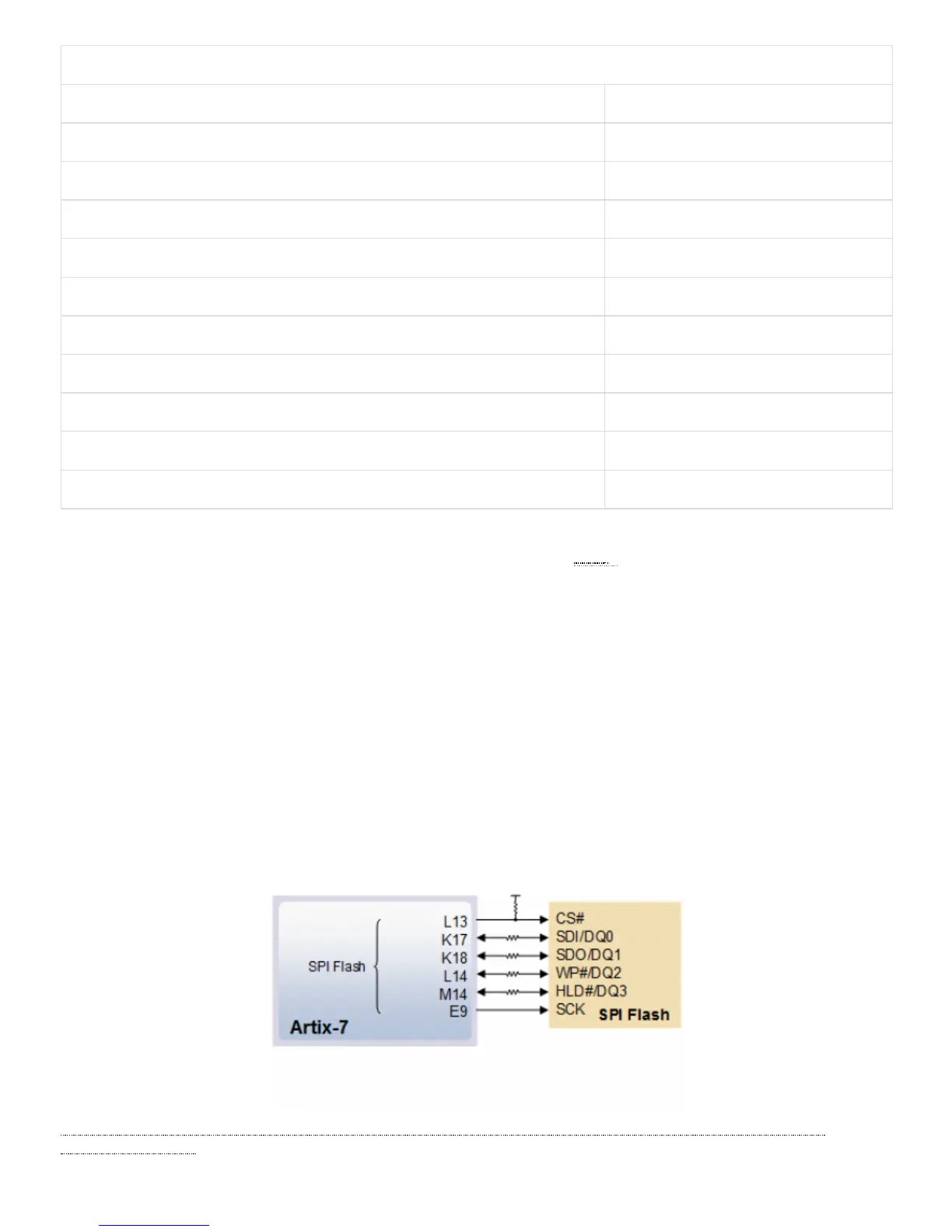
FPGA configuration files can be written to the Quad-SPI Flash (Spansion part number S25FL128S), and mode settings are available to
cause the FPGA to automatically read a configuration from this device at power on. An Artix-7 100T configuration file requires just less
than four MiB (mebibyte) of memory, leaving about 77% of the flash device available for user data. Or, if the FPGA is getting configured
from another source, the whole memory can be used for custom data.
The contents of the memory can be manipulated by issuing certain commands on the SPI bus. The implementation of this protocol is
outside the scope of this document. All signals in the SPI bus except SCK are general-purpose user I/O pins after FPGA configuration.
SCK is an exception because it remains a dedicated pin even after configuration. Access to this pin is provided through a special FPGA
primitive called STARTUPE2.
NOTE: Refer to the manufacturer’s data sheets² and Xilinx user guides³ for more information.
(https://reference.digilentinc.com/_detail/reference/programmable-logic/nexys-a7/n4f.png?id=reference%3Aprogrammable-logic%3Anexys-
a7%3Areference-manual) Figure 3.2.1 Nexys A7 DDR SPI Flash Pin-out
3.2 Quad-SPI Flash