https://reference.digilentinc.com/reference/programmable-logic/nexys-a7/reference-manual 23/30
JA7: D17 JB7: E16 JC7: E7 JD7: H2 JXADC7: A14 (AD3N)
JA8: E17 JB8: F13 JC8: J3 JD8: G4 JXADC8: A16 (AD10N)
JA9: F18 JB9: G13 JC9: J4 JD9: G2 JXADC9: B17 (AD2N)
JA10: G18 JB10: H16 JC10: E6 JD10: F3 JXADC10: A18 (AD11N)
Digilent produces a large collection of Pmod accessory boards that can attach to the Pmod expansion connectors to add ready-made
functions like A/D’s, D/A’s, motor drivers, sensors, as well as other functions. See www.digilentinc.com (http://www.digilentinc.com) for
more information.
The on-board Pmod expansion connector labeled “JXADC” is wired to the auxiliary analog input pins of the FPGA. Depending on the
configuration, this connector can be used to input differential analog signals to the analog-to-digital converter inside of the Artix-7 (XADC).
Any or all pairs in the connector can be configured either as analog input or digital input-output.
The Dual Analog/Digital Pmod on the Nexys A7 differs from the rest in the routing of its traces. The eight data signals are grouped into
four pairs, with the pairs routed closely coupled for better analog noise immunity. Furthermore, each pair has a partially loaded anti-alias
filter laid out on the PCB. The filter does not have capacitors C60-C63. In designs where such filters are desired, the capacitors can be
manually loaded by the user.
NOTE: The coupled routing and the anti-alias filters might limit the data speeds when used for digital signals.
The XADC core within the Artix-7 is a dual channel 12-bit analog-to-digital converter capable of operating at 1 MSPS. Either channel can
be driven by any of the auxiliary analog input pairs connected to the JXADC header. The XADC core is controlled and accessed from a user
design via the Dynamic Reconfiguration Port (DRP). The DRP also provides access to voltage monitors that are present on each of the
FPGA’s power rails, and a temperature sensor that is internal to the FPGA. For more information on using the XADC core, refer to the
Xilinx document titled “7 Series FPGAs and Zynq-7000 All Programmable SoC XADC Dual 12-Bit 1 MSPS Analog-to-Digital Converter.”
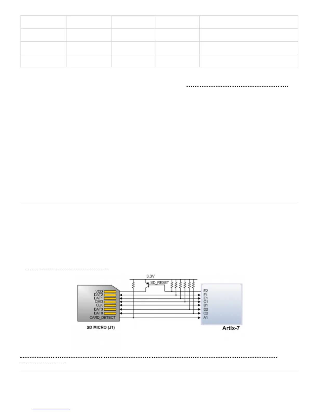
The Nexys A7 provides a microSD slot for both FPGA configuration and user access. The on-board Auxiliary Function microcontroller
shares the SD card bus with the FPGA. Before the FPGA is configured the microcontroller must have access to the SD card via SPI. Once
a bit file is downloaded to the FPGA (from any source), the microcontroller power cycles the SD slot and relinquishes control of the bus.
This enables any SD card in the slot to reset its internal state machines and boot up in SD native bus mode. All of the SD pins on the
FPGA are wired to support full SD speeds in native interface mode, as shown in Figure 11.1. The SPI is also available, if needed. Once
control over the SD bus is passed from the microcontroller to the FPGA, the SD_RESET signal needs to be actively driven low by the
FPGA to power the microSD card slot. For information on implementing an SD card controller, refer to the SD card specification available
at www.sdcard.org (http://www.sdcard.org).
(https://reference.digilentinc.com/_detail/reference/programmable-logic/nexys-a7/n4w.png?id=reference%3Aprogrammable-logic%3Anexys-
a7%3Areference-manual) Figure 11.1 Artix-7 microSD Card Connector Interface (PIC24 Connections not Shown)
10.1 Dual Analog/Digital Pmod
11 MicroSD Slot
12 Temperature Sensor
 Loading...