After Sales
Technical Documentation
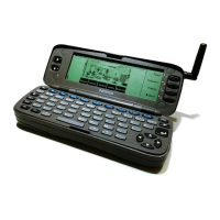
RAE/RAK–1N
PDA Hardware
Page 6 – 8
Original, 08/96
Table 3. DC characteristics of board to board connector Signals
Pin /
Type.
Line Symbol Mini-
mum
Typi-
cal /
Nomi-
nal (1)
Maxi-
mum
Notes
6 / UIF BACKLIGHT
0V 0.7V Output low, back-
lights off
Display
and key-
p
4.7V 4.85V 5.0V Output high, back-
lights on
-
mination
control
8 / PDA,
test
RBUSRxD
2.735
V
State ”1”
RBUS re-
ceived
0.4V State ”0”
CMT
3.6V 4.85V 5.0V State ”1”
RBUS re-
ceived
data to
0V 0.2V 0.7V State ”0”
-
ing CMT
FLASH
download
9 / PDA,
test
RBUSTxD
3.6V 4.85V 5.0V State ”1”
1 mA load
RBUS
trans-
mitted
0V 0.2V 0.7V State ”0”
data from
CMT
12 / UIF XPWRON
0V 0V 0.7V Input low, power on/
off
4.65V Floating when inac-
tive. A pull–up in
PSL+.
15 / SIM BUZZEROUT
0V 0.7V Output low, buzzer
off
5.2V 7.2V 8.4V Output high, buzzer
on
20–17 /
COL(3:0)
0V 0.7V Input low
keypad
UIF
4.7V 4.85V 5.0V Input high
columns
27–24 /
UIF
UIF(3:0)
0V 0.7V Output/Input low
keypad
row lines/
4.7V 4.85V 5.0V Output/Input high
display
data lines
28 / UIF UIF4
0V 0.7V Output/Input low
keypad
row
4.7V 4.85V 5.0V Output/Input high
strobe for
LCD driver
 Loading...