After Sales
Technical Documentation
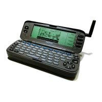
RAE–1N
Schematics
Page 10 – 2
Original 04/97
CONTENTS– Schematics
Page No
PDA version 13a
Figure 1 PDA Block Diagram 10–3. . . . . . . . . . . . . . . . . . . . . . . . . . . . . . . . . . . . . .
Figure 2 PDA Power Unit –PWRU 10–4. . . . . . . . . . . . . . . . . . . . . . . . . . . . . . . . .
Figure 3 PDA Serial Interface – SIRU 10–5. . . . . . . . . . . . . . . . . . . . . . . . . . . . . . .
Figure 4 PDA MCU and Memory – PROCU 10–6. . . . . . . . . . . . . . . . . . . . . . . . . .
Figure 5 PDA EMIU 10–7. . . . . . . . . . . . . . . . . . . . . . . . . . . . . . . . . . . . . . . . . . . . . .
Figure 6 Keyboard matrix 10–8. . . . . . . . . . . . . . . . . . . . . . . . . . . . . . . . . . . . . . . . . .
Figure 7 PDA Memory 10–9. . . . . . . . . . . . . . . . . . . . . . . . . . . . . . . . . . . . . . . . . . . .
Figure 8 PDA Component Layout 10–10. . . . . . . . . . . . . . . . . . . . . . . . . . . . . . . . . .
GSM version 09
Figure 9. CMT Component Layout – Bottom 10–11. . . . . . . . . . . . . . . . . . . . . . .
Figure 10 CMT Component Layout – Top 10–12. . . . . . . . . . . . . . . . . . . . . . . . . .
Figure 11 Baseband Circuit Diagram – PWRU 10–13. . . . . . . . . . . . . . . . . . . . . .
Figure 12 Baseband Circuit Diagram – MCM1 10–14. . . . . . . . . . . . . . . . . . . . . .
Figure 13 Baseband Circuit Diagram – MCM2 10–15. . . . . . . . . . . . . . . . . . . . . .
Figure 14 RF / TX Circuit Diagram 10–16. . . . . . . . . . . . . . . . . . . . . . . . . . . . . . . . .
Figure 15 RF / RX Circuit Diagram 10–17. . . . . . . . . . . . . . . . . . . . . . . . . . . . . . . .
Figure 16 UIF Schematic (v10) 10–18. . . . . . . . . . . . . . . . . . . . . . . . . . . . . . . . . . . .
Figure 17 UIF Component Layout (v10) 10–19. . . . . . . . . . . . . . . . . . . . . . . . . . . . .
PCN version 05
Figure 18. Component Layout – Bottom 10–20. . . . . . . . . . . . . . . . . . . . . . . . . . . .
Figure 19 Component Layout – Top 10–21. . . . . . . . . . . . . . . . . . . . . . . . . . . . . . .
Figure 20 RF / TX Circuit Diagram 10–22. . . . . . . . . . . . . . . . . . . . . . . . . . . . . . . . .
Figure 21 RF / RX Circuit Diagram 10–23. . . . . . . . . . . . . . . . . . . . . . . . . . . . . . . .
Figure 22 UIF Schematic (v1) 10–24. . . . . . . . . . . . . . . . . . . . . . . . . . . . . . . . . . . . .
Figure 23 UIF Component Layout (v 1) 10–25. . . . . . . . . . . . . . . . . . . . . . . . . . . . .
 Loading...