Hardware description
To ensure that only one of the power sources are used on the board at a time, power switches are
implemented on each of them as shown in Figure 9: Power sources and switches on page 15. These
switches prioritize the supply sources in the following manner:
1. USB
2. P15
3. P28
This means that if power is connected to more than one the interfaces, the higher priority interface will be
chosen to supply the board.
The supply voltage is then routed through the ON/OFF switch (SW9) to the common rail VSUPPLY, which
acts as the source for the supply voltage regulators for the circuitry on the board.
The supply flows from VOUT to VIN, which is correct. The body diode of the internal transistor powers the
VSUPPLY net, which supplies the gates controlling the enable signal of the switches.
The power switches will introduce a small voltage drop between the power source connected to the board
and the VSUPPLY. To avoid this, the power switches can be bypassed by shorting one of the solder bridges
as shown in the table:
Power source Power switch bypass Voltage level
USB connector (J4) SB24 5 V
External supply (P28) SB36 3.0 V–5.5 V
VIN 3–5 V (P15) SB4 3.0 V–5.5 V
Table 2: Bypassing power switch
Note: Connect only one power source at a time in this case. Shorting the solder bridges removes
the reverse voltage protection.
4.3.1 nRF9160 supply
The nRF9160 has a supply range of 3.0–5.5 V and is therefore powered by the VSUPPLY rail directly.
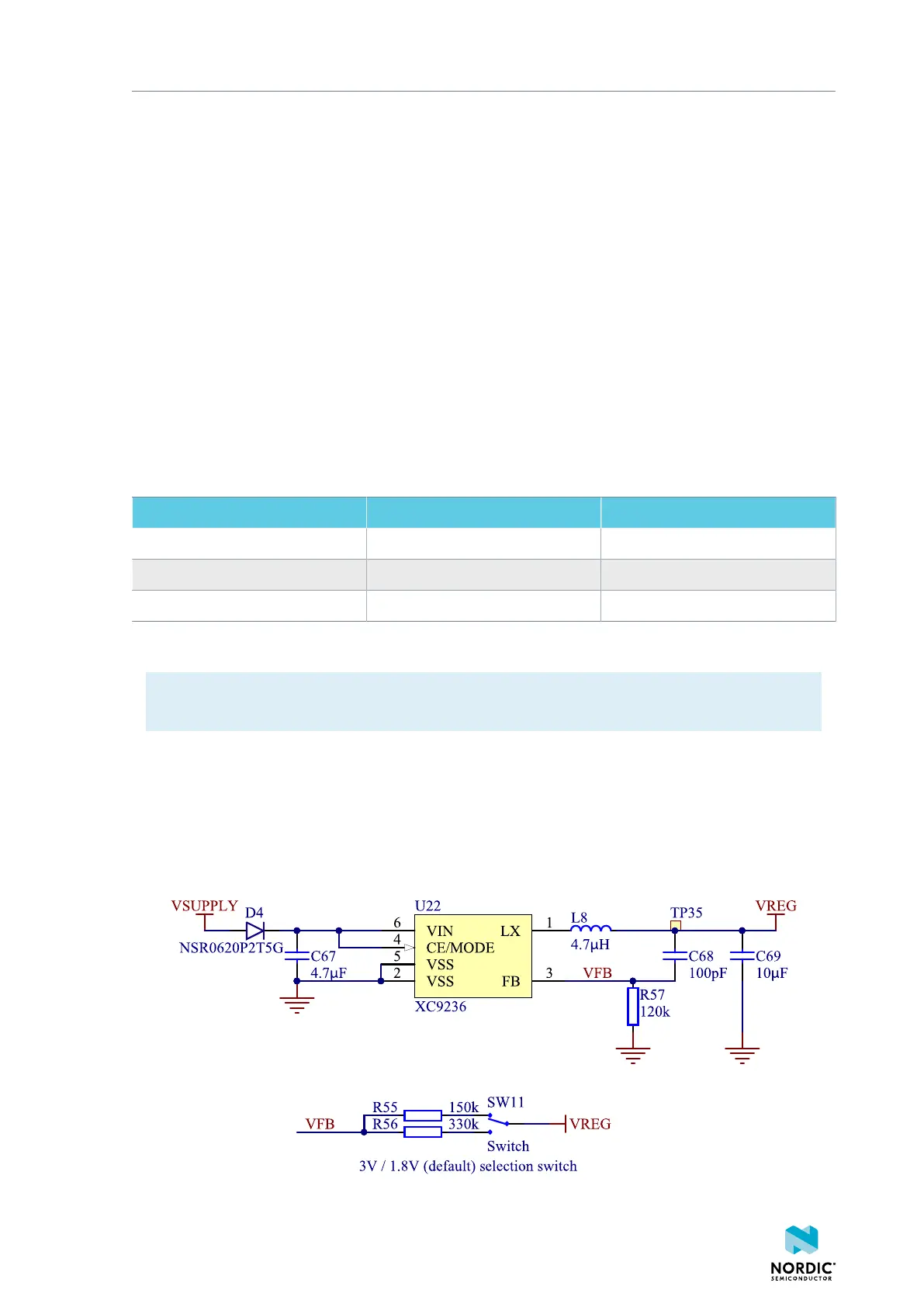
4.3.2 VDD supply rail
VDD is the main supply for the rest of the circuitry on the board. It is regulated down from VSUPPLY by a
buck regulator (U22).
Figure 10: VDD buck regulator and selection switch
4418_1216 v0.9.1
16
 Loading...