Hardware description
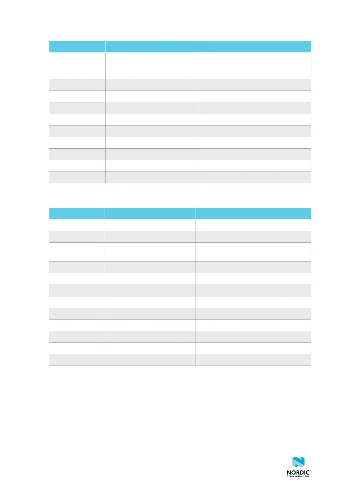
Pin number Signal Description
1 SWD0_SELECT Voltage supply from the external target,
used as voltage detect input to the interface
MCU
2 SWD0_SWDIO Serial Wire Debug (SWD) data line
3 GND Ground
4 SWD0_SWDCLK SWD clock line
5 GND Ground
6 SWD0_SWO Serial Wire Output (SWO) line
7 N.C. Not used
8 N.C. Not used
9 N.C. Not used
10 SWD0_RESET Reset
Table 7: Pinout of connector P22 for programming external targets
Pin number Signal Description
1 N.C. Not used
2 VDD Used for VDD voltage
3 SWD1_SELECT Voltage supply from the external target, used
as voltage detect input to the interface MCU
4 SWD1_SWDIO Serial Wire Debug (SWD) data line
5 SWD1_SWDCLK SWD clock line
6 SWD1_SWO Serial Wire Output (SWO) line
7 SWD1_RESET Reset line
8 N.C. Not used
9 VIN3-5V Voltage supply
9 VDD_HV Used for current measurement
10 VDD_HV’ Used for current measurement
12 VIO_REF GPIO voltage reference input
Table 8: Pinout of connector P15 for programming target on shields
4.11 Signal routing switches
A number of the GPIO signals of the nRF9160 are routed through analog switches for use for onboard
functionality or having them available on the pin headers for external circuitry or Arduino type shields.
4.11.1 Interface MCU disconnect switches
The IF MCU DISCONNECT mode can be enabled using the switches shown in the schematics.
4418_1216 v0.9.1
27
 Loading...