Power
NVIDIA Jetson TX2 NX DG-10141-001_v1.1 | 14
Power Rail Discharge
To satisfy the power down sequencing requirement and prevent unwanted back drive from the
carrier board to the module, the following must be true:
The carrier board 3.3V power supply that powers any module I/O must be off within 1.5 ms
of
SYS_RESET* assertion.
The 1.8V power supply that powers any module I/O must be off within 4 ms.
The power rails should be fully discharged before attempting to power back up.
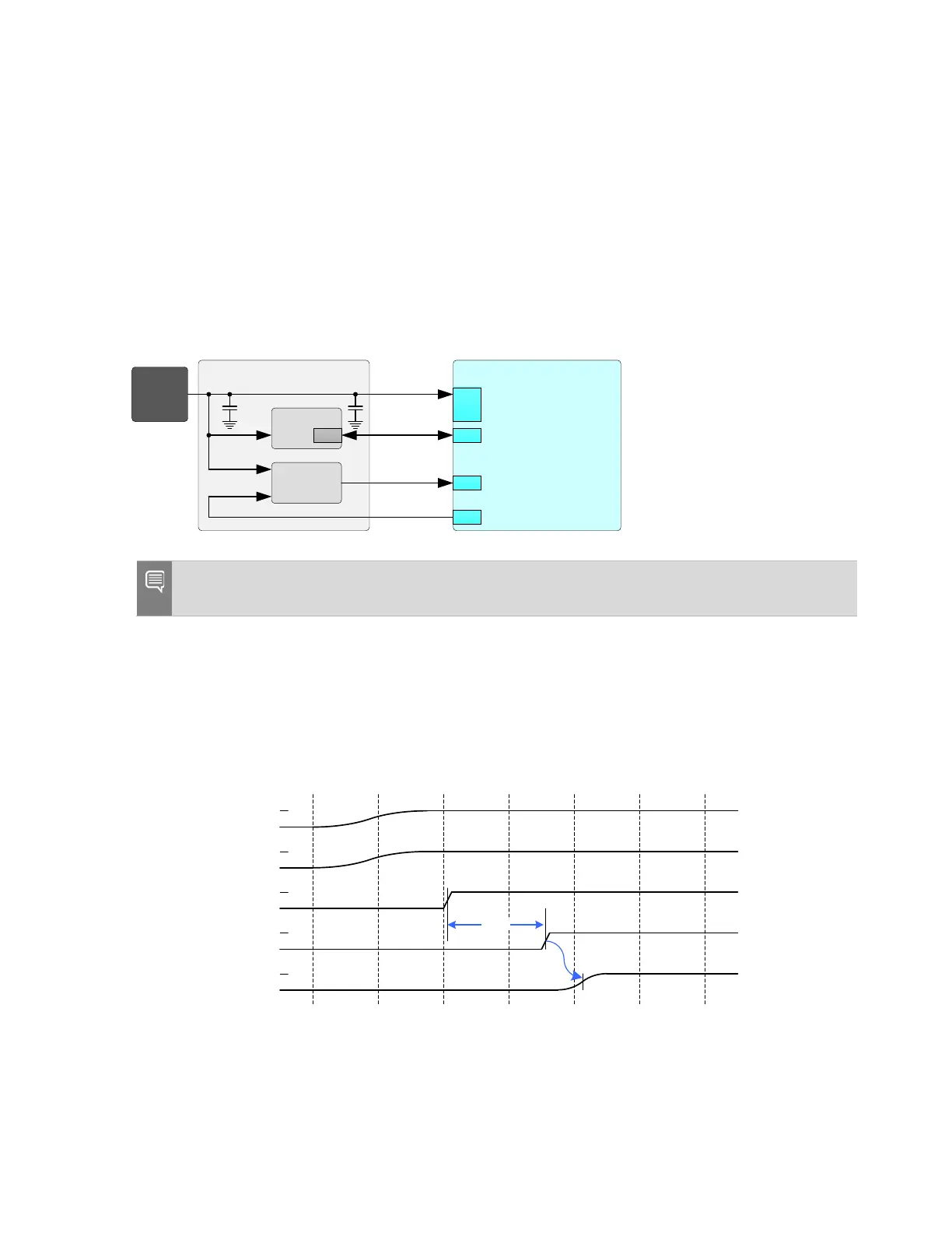
Figure 5-2. System Power and Control Block Diagram
Carrier Board
Main 5V
Power
Source
Sup plies
Jetson
Power
Logic
POWER_EN
251
↓
260
237
233
SHUTDOWN_REQ*
239
SYS_RESET*
VDD_IN
EN
Note: Designs which implement an eFUSE or current limiting device on the input power rail of
the module should select a part that DOES NOT limit reverse current.
5.1.2 Power Sequencing
The following figures show the power sequencing for the Jetson TX2 NX module.
Figure 5-3. Power Up Sequence (No Power Button – Auto Power-On)
POWER_E N
VDD_IN
Carrier Board Supplies
SYS_RESET*
SHUT DOW N_REQ*
~8 2ms