Display
NVIDIA Jetson TX2 NX DG-10141-001_v1.1 | 35
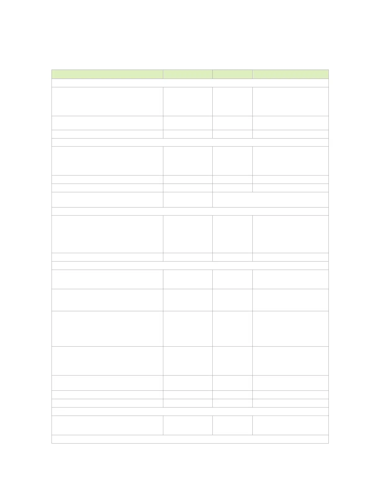
Table 7-7. eDP/DP Main Link Signal Routing Requirements including
DP_AUX
Parameter Requirement Units Notes
Specification
Max data rate / Min UI
R
1.62 / 617
2.7 / 370
5.4 / 185
Gbps / ps
Per data lane
Number of loads / topology 1 load
Point-Point, differential,
unidirectional
Termination 100 Ω On die at TX/RX
Electrical Spec
IL
0.7
1.2
2.4
dB @ 0.81GHz
dB @ 1.35GHz
dB @ 2.7GHz
Resonance dip frequency >8 GHz
TDR dip >85 Ω @ Tr-200ps (10%-90%)
FEXT <= -40dB @ DC
<= -30dB @ 2.7GHz
See Figure 7-4
Impedance
Trace impedance (Diff pair) 90-100
85
Ω (±15%)
90Ω–100Ω is the spec. target. 85Ω
is an implementation option (Zdiff
does not account for trace coupling)
85Ω is preferable as it can provide
better trace loss characteristic
performance. See Note 1.
Reference plane
Trace Length, Spacing and Skew
Trace loss characteristic: < 0.81 dB/in
@ 2.7GHz. The following max length
is derived based on this
characteristic. See Note 2.
Max PCB via dist. from connector
No requirement
7.63 (0.3)
mm (in)
Max trace length/delay from Jetson TX2 NX TX to
connector
(Stripline / Microstrip)
(Stripline)
(Microstrip, 5x / 7x)
215 (1138)/215 (975)
102 (700)
89 (525) / 102 (600)
mm (ps)
175ps/inch assumption for stripline,
150ps/inch for microstrip.
Trace spacing (pair-pair)
Stripline
Microstrip (
)
Microstrip (
)
3x
4x
5x to 7x
dielectric
Trace spacing (Main link to AUX)
Stripline/Microstrip
3x / 5x
dielectric
Max intra-pair (within pair) skew 0.15 (1) mm (ps) See Note 2
Maxinter-pair (pair-pair) skew 150 ps See Note 3
Via
Max
transition via distance < 1x diff pair pitch
For signals switching reference
layers, add symmetrical
stitching via near signal vias.
Via Structure