USB and PCI Express
NVIDIA Jetson TX2 NX DG-10141-001_v1.1 | 17
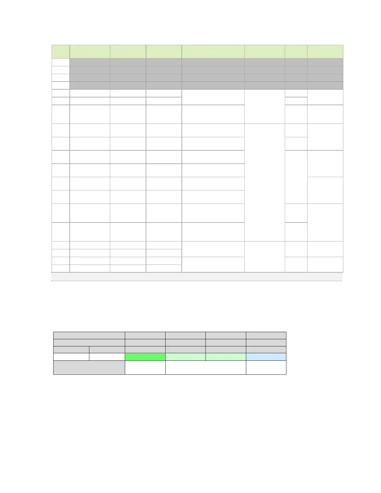
Pin # Module Pin Name
Jetson TX2 NX
Function
Tegra X2 Signal Usage/Description
Usage on DevKit
Carrier Board
Direction Pin Type
148 PCIE0_TX2_N RSVD − Reserved M.2 Key M − −
150 PCIE0_TX2_P RSVD − Reserved M.2 Key M − −
154 PCIE0_TX3_N RSVD − Reserved M.2 Key M − −
156 PCIE0_TX3_P RSVD − Reserved M.2 Key M − −
160 PCIE0_CLK_N PCIE0_CLK_N PEX_CLK1N
PCIe #0 Reference Clock (PCIe
Ctrl #0)
M.2 Key M
PCIe PHY
162 PCIE0_CLK_P PCIE0_CLK_P PEX_CLK1P
180 PCIE0_CLKREQ* PCIE0_CLKREQ*
PEX_L0_
CLKREQ_N
PCIE #0 Clock Request (PCIe
Ctrl #0). 47kΩ pull-up to 3.3V
on the module.
Bidir Open Drain 3.3V
167
(PCIE1_RX0_N)
RSVD
PCIE1_RX0_N PEX_RX0N
PCIe 1 Receive 0– (PCIe Ctrl #2
Lane 0)
M.2 Key E
Input
PCIe PHY
169
(PCIE1_RX0_P)
RSVD
PCIE1_RX0_P PEX_RX0P
PCIe 1 Receive 0+ (PCIe Ctrl #2
Lane 0)
Input
172
(PCIE1_TX0_N)
RSVD
PCIE1_TX0_N PEX_TX0N
PCIe 1 Transmit 0– (PCIe Ctrl
#2 Lane 0)
Output
PCIe PHY
174
(PCIE1_TX0_P)
RSVD
PCIE1_TX0_P PEX_TX0P
PCIe 1 Transmit 0+ (PCIe Ctrl
#2 Lane 0)
173
(PCIE1_CLK_N)
RSVD
PCIE1_CLK_N PEX_CLK3N
PCIe 1 Reference Clock– (PCIe
Ctrl #2)
PCIe PHY
175
(PCIE1_CLK_P)
RSVD
PCIE1_CLK_P PEX_CLK3P
PCIe 1 Reference Clock+ (PCIe
Ctrl #2)
182
(PCIE1_CLKREQ*)
RSVD
PCIE1_CLKREQ*
PEX_L2_
CLKREQ_N
PCIE 1 Clock Request (PCIe
Ctrl #2). 47kΩ pull-up to 3.3V
on the module.
Input
Open Drain 3.3V
183 (PCIE1_RST*) RSVD
PCIE1_RST* PEX_L2_RST_N
PCIe 1 Reset (PCIe Ctrl #2).
4.7kΩ pull-up to 3.3V on the
module.
Output
161 USBSS_RX_N USBSS_RX_N PEX_RX1N
USB SS Receive (USB 3.0 Ctrl
#1)
USB Hub
Input USB SS PHY
163 USBSS_RX_P USBSS_RX_P PEX_RX1P
166 USBSS_TX_N USBSS_TX_N PEX_TX1N
USB SS Transmit (USB 3.0 Ctrl
#1)
Output USB SS PHY
168 USBSS_TX_P USBSS_TX_P PEX_TX1P
Notes: In the Type/Dir column, Output is from Jetson TX2 NX. Input is to Jetson TX2 NX. Bidir is for Bidirectional signals.
Table 6-3 lists the mapping options for Jetson TX2 NX.
Table 6-3. Jetson TX2 NX USB 3.0 and PCIe Lane Mapping Configurations
Usage on DevKit Carrier
Board