Audio
NVIDIA Jetson TX2 NX DG-10141-001_v1.1 | 56
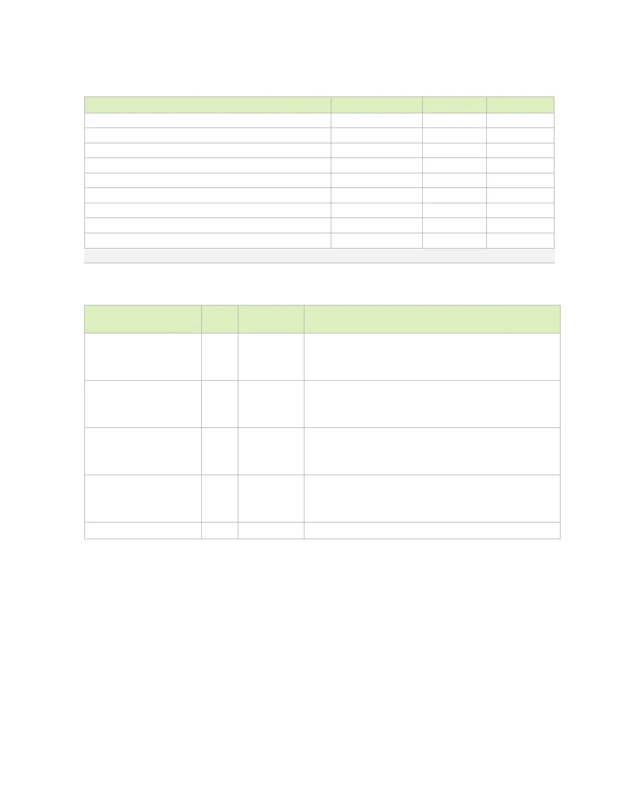
Table 10-2. Interface Signal Routing Requirements
Parameter Requirement Units Notes
Configuration / device organization 1 load
Max loading 8 pF
Reference plane GND
Breakout region impedance Min width/spacing
Trace impedance 50 Ω ±20%
Via proximity (signal to reference) < 3.8 (24) mm (ps) See note
Trace spacing Microstrip or Stripline 2x dielectric
Max trace length/delay ~22 (3600) In (ps)
Max trace length/delay skew between SCLK and
OUT/IN ~1.6 (250) In (ps)
Note: Up to four signal vias can share a single
return via.
Table 10-3. Audio Signal Connections
Module Pin Name
(Function)
Type Termination Description
I2S[1:0]_SCLK
GPIO05 (I2S2_SCLK)
GPIO06 (I2S3_SCLK)
I/O I2S Serial Clock: Connect to I2S/PCM CLK pin of audio device.
I2S[1:0]_FS
GPIO04 (I2S2_FS)
SPI1_CS1* (I2S3_FS)
I/O
I2S Frame Select (Left/Right Clock): Connect to corresponding pin
of audio device.
I2S[1:0]_DOUT
GPIO02 (I2S2_DOUT)
GPIO12 (I2S3_DOUT)
I/O
I2S Data Output: Connect to data input pin of audio device.
I2S[1:0]_DIN
GPIO03 (I2S2_DIN)
GPIO10 (I2S3_DIN)
I I2S Data Input: Connect to data output pin of audio device.
Audio Codec Master Clock: Connect to clock pin of audio codec.