USB and PCI Express
NVIDIA Jetson TX2 NX DG-10141-001_v1.1 | 18
6.1 USB
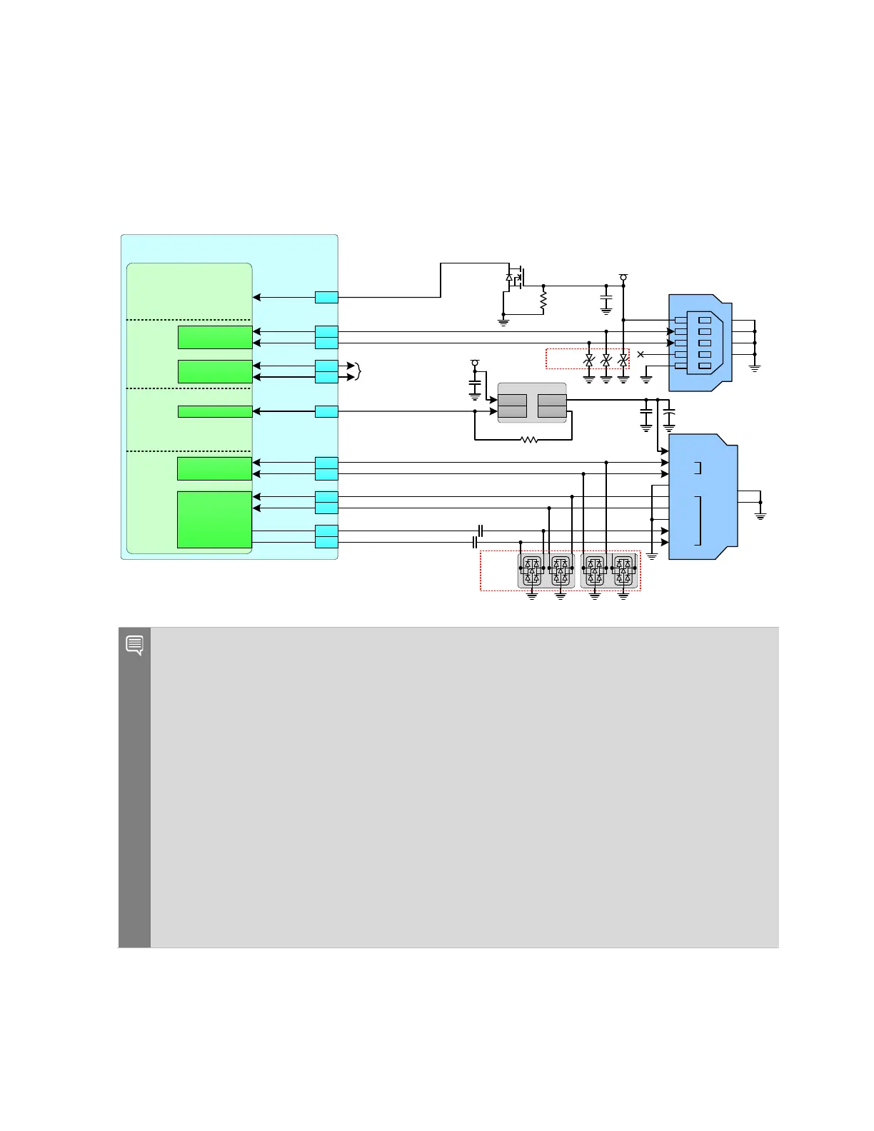
Figure 6-1 shows the USB connection example.
Figure 6-1. USB Connection Example
Jetson
Tegra
USB 2.0
USB0_ DN
USB0_ DP
PEX_RX1_N
PEX_RX1_P
PEX_TX1_N
PEX_TX1_P
USB 3.0
& P EX
USB1_ DN
USB1_ DP
USB2_ DN
USB2_ DP
GP IO 00
USB1_D_N
USB1_D_P
USB S S_ RX_ N
USB S S_ RX_ P
USB S S_ TX_ N
USB S S_ TX_ P
GP IO x
USB0_D_N
USB0_D_P
USB2_D_N
USB2_D_P
USB_VBUS_EN0
UARTCAM
Ava ilable: Used
for M.2 Module
on DevKi t Car rier
Board
*
111
109
123
121
117
115
166
168
161
163
Load Switch
EN OC
IN OUT
100Ω
0. 1 uF
0. 1 uF
VDD_5V_IN
USB0_VBUS_DET
87
Enable / O ver-Current Status
VDD_5V_USB
1M
Ω
G
S
D
4.7uF
VBUS
DN
DP
ID
GND
SH1
SH2
SH3
SH4
MSP5.0A
-M3/89A
T PD4E 05U06
VBUS
DN
DP
GND
RX_ N
RX_ P
GND
TX _N
TX _p
USB 2.0
USB 3.0
TAB
TAB
USB
Micro B
USB SS
Type A
Notes:
1. AC capacitors should be located close to either the USB connector, or the Jetson TX2 NX pins.
2. For USB 3.0 IF shown above (USBSS_TX/RX), AC caps are required on the TX lines. If routed
directly to a peripheral, AC caps are needed on the peripheral TX lines as well. The AC caps
are recommended to be located near the Jetson TX2 NX connector pins, although locating the
caps near the peripheral RX pins is acceptable.
3. USB0 must be available to use as USB Device for USB Recovery Mode.
4. USB0 VBUS Detect, if required for USB Device Mode, connects to an available GPIO. This
signal is not required if the connector (Micro B in this case) is only used for USB Recovery
Mode.
5. The load switch supplying VBUS should have over current protection. In Figure 6-1 this is
supported by routing the over current (OC) pin of the load switch to the GPIO00
(USB_VBUS_EN0) which is bidirectional and can be used to detect an over current condition.
6. Connector used must be USB Implementers Forum certified if USB 3.0 implemented.