NVIDIA Jetson TX2 NX DG-10141-001_v1.1 | 16
Chapter 6. USB and PCI Express
Jetson TX2 NX allows multiple USB 2.0, USB 3.0 and PCIe interfaces to be brought out of the
module.
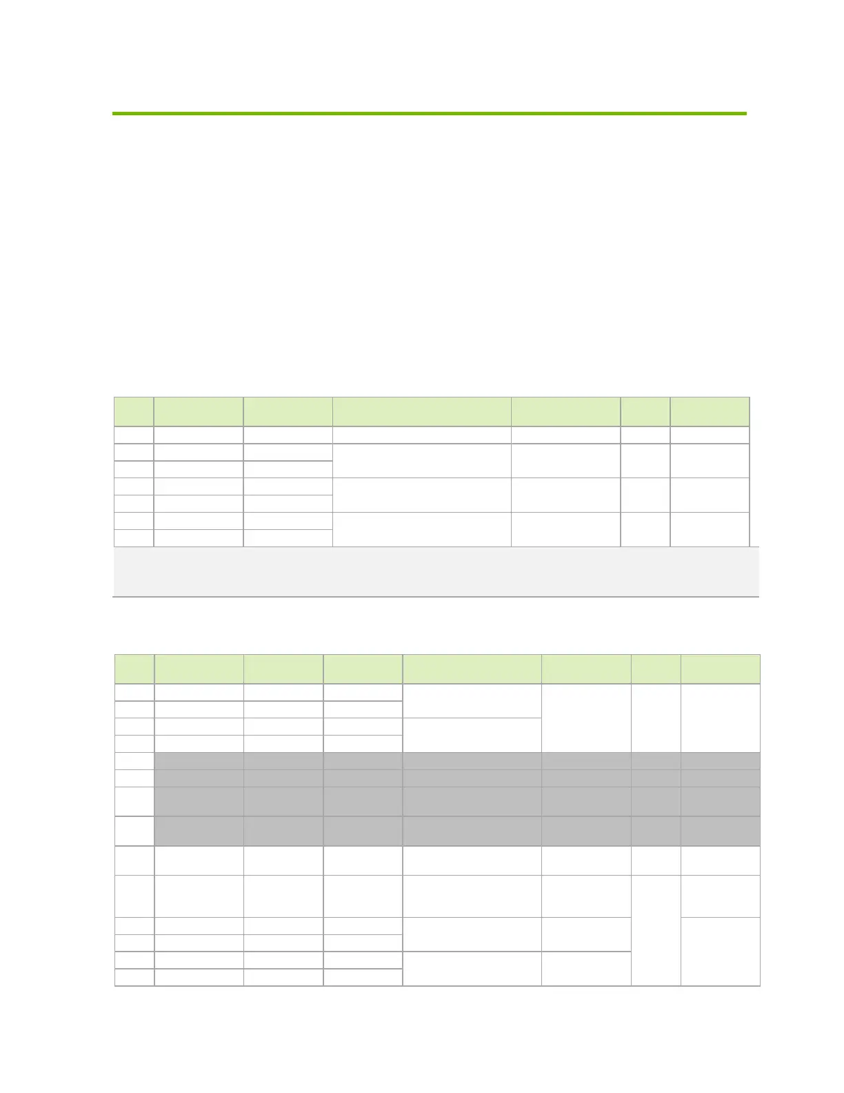
Table 6-1. Jetson TX2 NX USB 2.0 Pin Descriptions
Pin # Module Pin Name Tegra X2 Signal Usage/Description
Usage on DevKit
Carrier Board
Direction Pin Type
87 GPIO00 USB_VBUS_EN0 GPIO #0 (USB 0 VBUS Detect) USB 2.0 Micro B Input Open Drain, 1.8V
109 USB0_D_N USB0_DN
USB 2.0 Port 0 Data USB 2.0 Micro B Bidir USB PHY
111 USB0_D_P USB0_DP
115 USB1_D_N USB1_DN
USB 2.0 Port 1 Data USB Hub Bidir USB PHY
121 USB2_D_N USB2_DN
USB 2.0, Port 2 Data M.2 Key E Bidir USB PHY
123 USB2_D_P USB2_DP
Notes:
1. In the Type/Dir column, Output is from Jetson TX2 NX. Input is to Jetson TX2 NX. Bidir is for Bidirectional signals.
2. The direction of GPIO00 is true when used for this function. Otherwise as a GPIO, the direction is bidirectional.
Table 6-2. Jetson TX2 NX USB 3.0 and PCIe Pin Descriptions
Pin # Module Pin Name
Jetson TX2 NX
Function
Tegra X2 Signal Usage/Description
Usage on DevKit
Carrier Board
Direction Pin Type
131 PCIE0_RX0_N PCIE0_RX0_N PEX_RX4N
PCIe #0 Receive 0 (PCIe Ctrl #0
Lane 0)
M.2 Key M Input PCIe PHY
133 PCIE0_RX0_P PCIE0_RX0_P PEX_RX4P
137 PCIE0_RX1_N PCIE0_RX1_N PEX_RX2N
PCIe #0 Receive 1 (PCIe Ctrl #0
Lane 1)
139 PCIE0_RX1_P PCIE0_RX1_P PEX_RX2P
149 PCIE0_RX2_N RSVD - Reserved M.2 Key M - -
151 PCIE0_RX2_P RSVD - Reserved M.2 Key M - -
155
PCIE0_RX3_N
(RSVD)
RSVD − Reserved
M.2 Key M
− −
157
PCIE0_RX3_P
(RSVD)
RSVD − Reserved
M.2 Key M
− −
179 PCIE_WAKE* PCIE_WAKE* PEX_WAKE_N
PCIe Wake. 47kΩ pull-up to
3.3V on the module.
M.2 Key E & M Input Open Drain 3.3V
181 PCIE0_RST* PCIE0_RST* PEX_L0_RST_N
PCIe #0 Reset (PCIe Ctrl #0).
4.7kΩ pull-up to 3.3V on the
module.
M.2 Key M
Output
Open Drain 3.3V
134 PCIE0_TX0_N PCIE0_TX0_N PEX_TX4N
PCIe #0 Transmit 0 (PCIe Ctrl
#0 Lane 0)
M.2 Key M
PCIe PHY
136 PCIE0_TX0_P PCIE0_TX0_P PEX_TX4P
140 PCIE0_TX1_N PCIE0_TX1_N PEX_TX2N
PCIe #0
Lane 1)
M.2 Key M
142 PCIE0_TX1_P PCIE0_TX1_P PEX_TX2P