USB and PCI Express
NVIDIA Jetson TX2 NX DG-10141-001_v1.1 | 26
Parameter Requirement Units Notes
Voiding Voiding the plane directly under the pad
3-4 mils larger than the pad size is
recommended.
See Figure 6-8
General: See Chapter 15 for guidelines related to serpentine routing, routing over voids and noise coupling
Notes:
1. The PCIe spec. has 40-60Ω absolute min/max trace impedance, which can be used instead of the 50Ω, ± 15%.
2. If routing in the same layer is necessary, route group TX and RX separately without mixing RX/TX routes and keep distance between
nearest TX/RX trace and RX to other signals 3x RX-RX separation.
3. Longer trace lengths may be possible if the total trace loss is equal to or better than the target. If the loss is greater, the max trace
lengths will need to be reduced.
4. Do length matching before via transitions to different layers or any discontinuity to minimize common mode conversion.
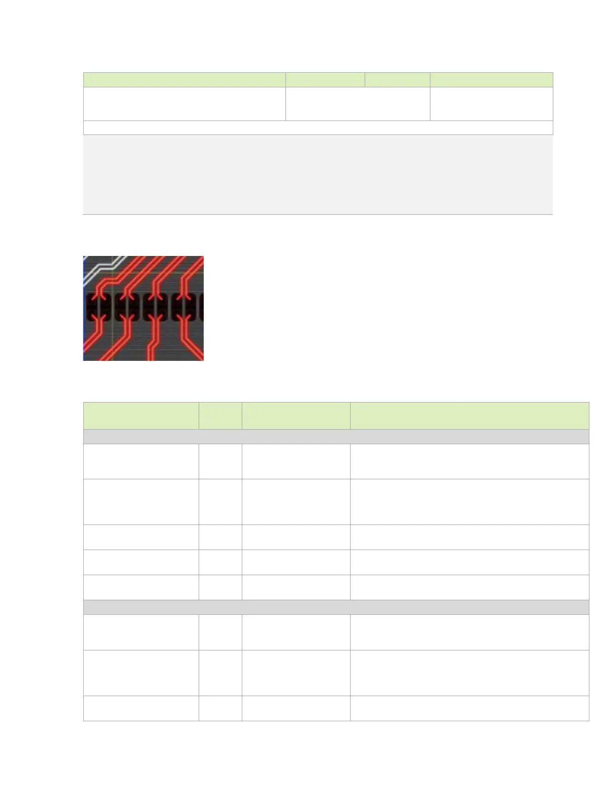
Figure 6-8. AC Cap Voiding
Table 6-10. PCIe Signal Connections
Module Pin Name
(Jetson TX2 NX Function)
Type Termination Description
PCIe Interface 0 (x2 – Controller #0)
PCIE0_TX1_N/P - Lane 1
PCIE0_TX0_N/P - Lane 0
DIFF
OUT
Series 0.1uF Capacitor Differential Transmit Data Pairs: Connect to TX_N/P pins of
PCIe connector or
pin of PCIe device through AC cap
according to supported configuration.
PCIE0_RX1_N/P - Lane 1
PCIE0_RX0_N/P - Lane 0
DIFF IN
Series 0.1uF capacitors
near Jetson TX2 NX pins or
device if device on main
PCB.
Differential Receive Data Pairs: Connect to RX_N/P pins of PCIe
connector or
pin of PCIe device through AC cap
according to supported configuration.
PCIE0_CLK_N/P DIFF
OUT
Differential Reference Clock Output: Connect to
REFCLK_N/P pins
of PCIe device/connector
PCIE0_CLKREQ* I 47kΩ pull-up to
on module
PCIe Clock Request for PCIE0_CLK:
Connect to
pins
on device/connector(s)
PCIE0_RST* O
4.7kΩ pull-up to
on module
Connect to
pins on device/connector(s)
PCIe Interface 1 (x1 – Controller #2)
PCIE1_TX0_N/P DIFF
OUT
Series 0.1uF Capacitor Differential Transmit Data Pair: Connect to TX_N/P pins of PCIe
connector or
pin of PCIe device through AC cap
according to supported configuration.
PCIE1_RX0_N/P DIFF IN Series 0.1uF capacitors
near Jetson TX2 NX pins or
device if device on main
PCB.
Differential Receive Data Pair: Connect to RX_N/P pins of PCIe
connector or
pin of PCIe device through AC cap
according to supported configuration.
PCIE1_CLK_N/P
DIFF
OUT
Differential Reference Clock Output: Connect to
REFCLK_N/P pins
of PCIe device/connector