4.3.
MCU Clock Configuration
There is an external 40MHz crystal connected to the MCU Fast External Oscillator (FXOSC)
pins EXTAL and XTAL.
There is also a 32.768 crystal connected to the MCU Slow External Oscillator (SXOSC) pins
OSC32K_EXTAL and OSC32K_XTAL. This can be used for accurate time keeping.
There are 2 pads PG6 and PG7 (located just below the MCU) on the LCEVB to facilitate
measurement of the CLKOUT1 and CLKOUT0 signals.
Note – there is no external clock input on the LCEVB
4.4.
Debug Connector (P1)
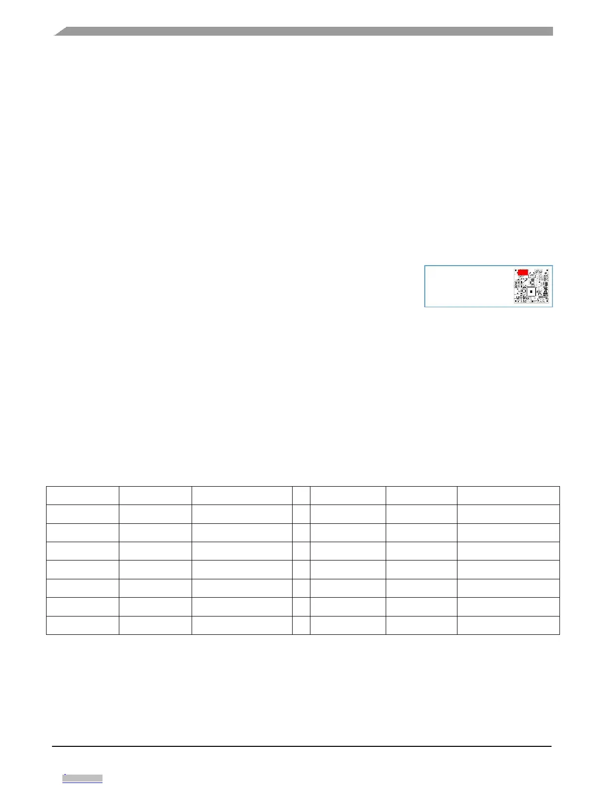
The JTAG debug
connectors is
located in the top left
corner of the LCEVB
The LCEVB has a single 14-pin keyed JTAG connector for connection to an external debugger.
Before attaching or removing the debug cable from the LCEVB remove power from the EVB to
prevent damage to the LCEVB or debug hardware.
4.4.1.
Debug Connector Pinout
The following tables list the pinout for the JTAG connector used on the LCEVB
Table 3. 14-Pin JTAG Debug Connector Pinout
TDI, TDO and TMS have 10K pullup resistors on the LCEVB. TCLK has a 10K pulldown (R147) to
facilitate STANDBY exit without any additional code (at the sacrifice of slightly higher STANDBY
current), however this can be changed to a pullup if required by removing R147 and fitting the resistor
on R56.
MPC5748G Low Cost EVB User Guide, Rev. 1, 08/2016
10 NXP Semiconductors
Downloaded from Arrow.com.Downloaded from Arrow.com.Downloaded from Arrow.com.Downloaded from Arrow.com.Downloaded from Arrow.com.Downloaded from Arrow.com.Downloaded from Arrow.com.Downloaded from Arrow.com.Downloaded from Arrow.com.Downloaded from Arrow.com.