Communications & Memory Interfaces:
Table 4. JTAG Pins Pull State (from MPC5748G Reference Manual)
5. Communications & Memory Interfaces:
This section details the communication interface and storage peripherals that are implemented on
the LCEVB.
5.1.
CAN Interfaces (P2, P3)
The CAN circuitry is
located on the top
right edge of the
LCEVB
The LCEVB incorporates two identical CAN interface circuits connected to MCU CAN0 and CAN1
using MC33901 transceivers. Both transceivers are configured for high speed operation by pulling pin
8 to GND via a 4.7 kOhm resistor. There are test points to allow the Select pin to be driven high if
desired. The MC33901 is pin compatible with other CAN transceivers supporting full CAN FD data
rates.
For flexibility, the CAN transceiver I/O is connected to a 0.1” header (P2 for CAN0 / P3 for CAN1)
rather than using non-standard DB9 connectors. The pinout of these headers is shown below.
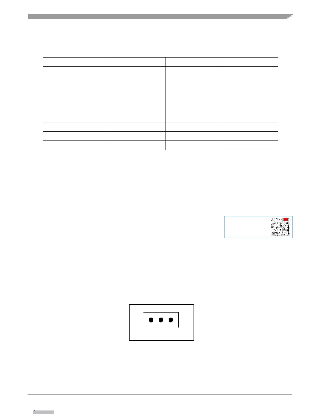
1
H L GND
Figure 5. CAN Physical Interface Connectors
MPC5748G Low Cost EVB User Guide, User Guide, Rev. 1, 08/2016
NXP Semiconductors 11
Downloaded from Arrow.com.Downloaded from Arrow.com.Downloaded from Arrow.com.Downloaded from Arrow.com.Downloaded from Arrow.com.Downloaded from Arrow.com.Downloaded from Arrow.com.Downloaded from Arrow.com.Downloaded from Arrow.com.Downloaded from Arrow.com.Downloaded from Arrow.com.