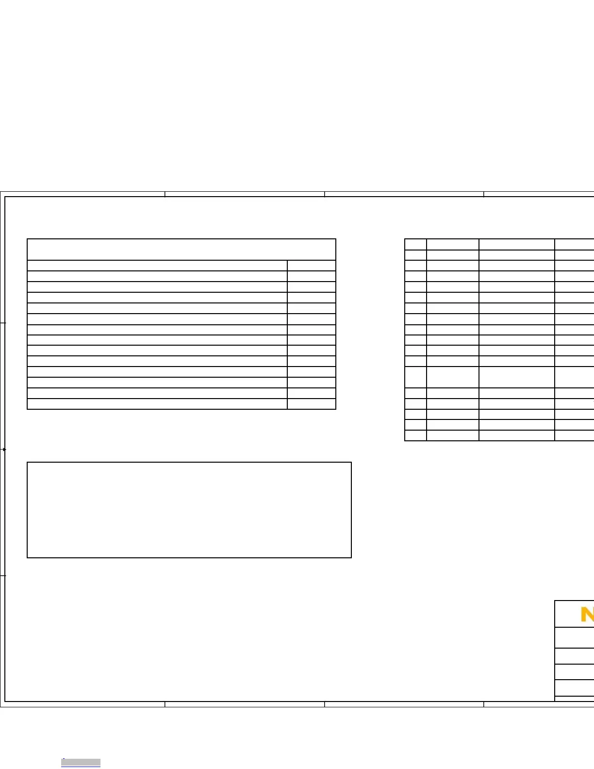
MPC5748G Low Cost Evaluation Board (MPC5748G-LCEVB)
Start of capture, Working version (256BGA)
Power - Main input and 3.3V regulator
Changed to 176 QFP Package and changed periperhal Matrix
Changes required for initial placement
Tidy Up, Replaced some "hard to source" components
Renumber and Back Annoted from Layout
Correction to GND on 3v3 Regulator circuit
Correction to CAN Test points
Few refdes changes after layout tweaks
Correction to user LED Refdes after re-number
Comms 2 - FTDI RS232 Interface
DNP Jumpers. 0 Ohm resistors added accross LIN jumpers
Comms 3 - USB Host Interface (device footprints only)
Prototype Manufacture Release
Comms 4 - Ethernet (MII Mode)
Prodn Build changes (LIN0 default to Slave, LIN1 Master only)
PN Changed to MPC5748G-LCEVB
User - Switches, LED's and Potentiometer
Change to JTAG Pulls to meet latest RM Spec
Changed RV1 current limit resistor. SW4 / SW5 refdes swap
Pull DOWN on TCLK to mitigate against STANDBY exit issue.
These schematics are provided for reference purposes only.
As such,NXP does not make any warranty, implied or otherwise, as to the
suitability of circuit design or component selection (type or value) used in
these schematics for hardware design using the NXP Calypso family of
Microprocessors. Customers using any part of these schematics as a
3 Different test points used in design:
basis for hardware design, do so at their own risk and NXP does not
TPVx - Through Hole Pad small
assume any liability for such a hardware design.
TPHx - Through Hile Pad Large (for standard 0.1" header).
- Surface Mount Wire Loop
- All components and board processes are to be ROHS compliant
- All small capacitors are 0402 unless otherwise stated
- All resistors are 0603 5% 0.1w unless otherwise stated. All zero ohm links are 0603
- All connectors and headers are denoted Px and are 2.54mm pitch unless otherwise stated
Automotive Microcontroller Applications
- All jumpers are denoted Jx. Jumpers are 2mm pitch
- Jumper default positions are shown in the schematics. For 3 way jumpers, default is always posn 1-2.
2 Pin jumpers generally have the "source" on pin 1.
- All switches are denoted SWx
This document contains information proprietary to NXP and shall not be used for engineering design,
- All test points (SMT wire loop style) are denoted TPx
without the express written permission of NXP Semiconductors.
- Test point Vias (just through hole pads) are denoted TPVx
procurement or manufacture in whole or in part Freescale AISG Applications, East Kilbride
Signals (ports) have not been routed via busses as this makes it harder to determine where each signal goes.
User notes are given throughtout the schematics.
Specific PCB LAYOUT notes are detailed in ITALICS
Friday, February 12, 2016
Downloaded from Arrow.com.Downloaded from Arrow.com.Downloaded from Arrow.com.Downloaded from Arrow.com.Downloaded from Arrow.com.Downloaded from Arrow.com.Downloaded from Arrow.com.Downloaded from Arrow.com.Downloaded from Arrow.com.Downloaded from Arrow.com.Downloaded from Arrow.com.Downloaded from Arrow.com.Downloaded from Arrow.com.Downloaded from Arrow.com.Downloaded from Arrow.com.Downloaded from Arrow.com.Downloaded from Arrow.com.Downloaded from Arrow.com.Downloaded from Arrow.com.
 Loading...


