RFID System
User's Manual
SECTION 7
Characteristics According to Operating Conditions
SECTION 7
Appendices
137
Communications Time (Reference)
Processing blocks refer to the 8-byte memory areas expressed by RF Tag addresses @@@0 to @@@7 hex and @@@8 to @@@F
hex.
Processing blocks refer to the 32-byte memory areas expressed by RF Tag addresses @@00 hex to @@1F hex, @@20 hex to
@@3F hex,
, @@E0 hex to @@FF hex.
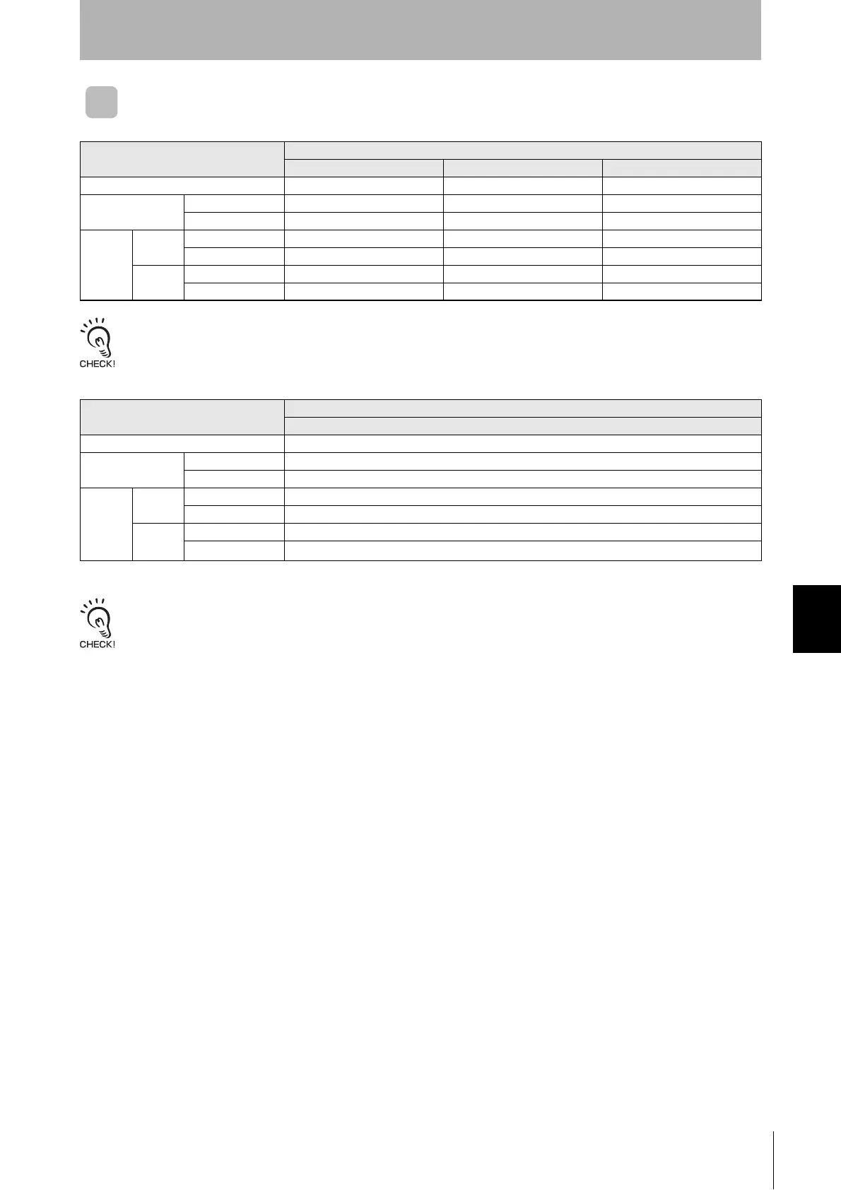
Communications time (ms)
V680-D1KP@@ V680-D2KF@@ V680-D8KF@@/-D32KF@@
READ 29.6 27.5 29.0
WRITE, BIT SET,
BIT CLEAR
With write verification 76.5 78.4 66.8
Without write verification 71.4 58.3 62.5
DATA FILL Normal
mode
With write verification 17.6 No. of processing blocks + 60 20.4 No. of processing blocks + 52 13.3 No. of processing blocks + 59
Without write verification 14.9 No. of processing blocks + 57 10.2 No. of processing blocks + 49 10.9 No. of processing blocks + 52
High-speed
mode
With write verification 14.9 No. of processing blocks + 51 14.7 No. of processing blocks + 49 8.8 No. of processing blocks + 41
Without write verification 12.1 No. of processing blocks + 47 7.5 No. of processing blocks + 41 7.6 No. of processing blocks + 40
Communications time (ms)
V680S-D8KF@@
READ 42
WRITE, BIT SET,
BIT CLEAR
With write verification 133
Without write verification 97
DATA FILL Normal
mode
With write verification 9.1 No. of processing blocks + 105.5
Without write verification 4.6 No. of processing blocks + 82.9
High-speed
mode
(See note.)
With write verification 9.1 No. of processing blocks + 105.5
Without write verification 4.6 No. of processing blocks + 82.9
Note: When using V680S-D8KF@@ RF Tags, the Normal Mode communications speed will be used even if the High-speed Mode is set.


 To Next Page