IC BLOCK DIAGRAMS AND TERMINAL DESCRIPTIONS -31
Q3601 : D707E001BRFP250 (32 bit Floating-Point Digital Signal Processor)
TERMINAL DESCRIPTION(3/3)
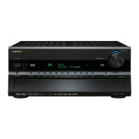
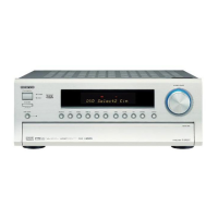
TX-SR876/SA876
Clocks
OSCIN 23 I 1.2-V OscillatorInput
OSCOUT 24 O 1.2-V OscillatorOutput
OSCVDD 25 PWR Oscillator 1.2-V VDD tap point (for filter only)
OSCVSS 22 PWR Oscillator VSS tap point (for filter only)
CLKIN 17 I Alternate clock input (3.3-V LVCMOS Input)
PLLHV 27 PWR PLL 3.3-V Supply Input (requires external filter)
Device Reset
RESET 14 I Device reset pin
Emulation/JTAG Port
TCK 35 I Test Clock
TMS 19 I Test Mode Select
TDI 28 I Test Data In
TDO 29 OZ Test Data Out
TRST 21 I Test Reset
EMU[0] 32 IO Emulation Pin 0
EMU[1] 34 IO Emulation Pin 1
Power Pins
Core Supply (CVDD)
IO Supply (DVDD)
Ground (VSS)
8, 16, 20, 33, 44, 53, 57, 65, 77, 85, 90, 101, 123, 128, 132
10, 31, 42, 50, 60, 68, 73, 81, 92, 103, 112, 125, 136
1, 6, 13, 15, 18, 26, 30, 36, 40, 47, 54, 62, 69, 72, 78, 82, 87, 95, 99, 106, 109, 114, 118, 124, 129, 133, 140
TYPE
SIGNAL NAME PIN NO. DESCRIPTION