A
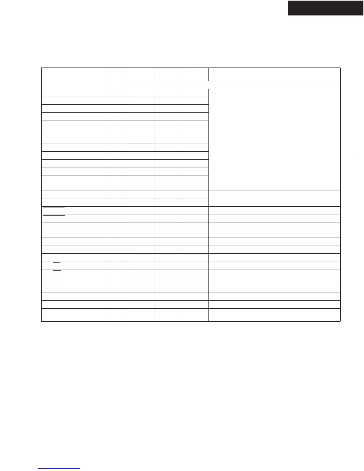
TERMINAL DESCRIPTION(2/5)
IC BLOCK DIAGRAMS AND TERMINAL DESCRIPTIONS -18
Q3401, Q3501: D790E001BZDH300 (Audio DSP)
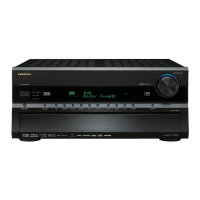
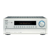
TX-SR876/SA876
BALL
SIGNAL NAME TYPE
(1)
PULL
(2)
GPIO
(3)
DESCRIPTION
NO.
External Memory Interface (EMIF) Address and Control
EM_A[0] J16 O - N
EM_A[1] J15 O - N
EM_A[2] K15 O - N
EM_A[3] L16 O - N
EM_A[4] L15 O - N
EM_A[5] M16 O - N
EM_A[6] M15 O - N EMIF Address Bus
EM_A[7] N16 O - N
EM_A[8] N15 O - N
EM_A[9] P16 O - N
EM_A[10] H15 O - N
EM_A[11] P15 O - N
EM_A[12] P12 O IPD N
EM_BA[0] G15 O - N
SDRAM Bank Address and Asynchronous Memory
Low-Order Address
EM_BA[1] H16 O - N
EM_CS[0]
F15 O - N SDRAM Chip Select
EM_CS[2]
E15 O - N Asynchronous Memory Chip Select
EM_CAS
R3 O - N SDRAM Column Address Strobe
EM_RAS F16 O - N SDRAM Row Address Strobe
EM_WE T3 O - N SDRAM Write Enable
EM_CKE T14 O - N SDRAM Clock Enable
EM_CLK R14 O - N SDRAM Clock
EM_WE_DQM[0] R4 O - N Write Enable or Byte Enable for EM_D[7:0]
EM_WE_DQM[1] T13 O - N Write Enable or Byte Enable for EM_D[15:8]
EM_WE_DQM[2]
P13 O IPU N Write Enable or Byte Enable for EM_D[23:16]
EM_WE_DQM[3]
R15 O IPU N Write Enable or Byte Enable for EM_D[31:24]
EM_OE D15 O - N SDRAM Output Enable
EM_RW
E16 O - N Asynchronous Memory Read/not Write
Asynchronous Wait Input (Programmable Polarity) or
EM_WAIT D14 I IPU N
Interrupt (NAND)
(1) TYPE column refers to pin direction in functional mode. If a pin has more than one function with different directions, the functions are
separated with a slash (/).
(2) PULL column:
IPD = Internal Pulldown resistor
IPU = Internal Pullup resistor
(3) If the GPIO column is 'Y', then in GPIO mode, the pin is configurable as an IO unless otherwise marked.