EasyManua.ls Logo

Panasonic KX-NS500AG User Manual

Panasonic KX-NS500AG
191 pages
To Next Page IconTo Next Page
Page #1 background imageLoading...
Page #1 background image
© Panasonic System Networks Co., Ltd. 2014
Unauthorized copying and distribution is a violation
of law.
ORDER NO. KMS1409096CE
Hybrid IP-PBX
Model No. KX-NS500AG
(for Argentina)

Table of Contents

Question and Answer IconNeed help?

Do you have a question about the Panasonic KX-NS500AG and is the answer not in the manual?

Panasonic KX-NS500AG Specifications

General IconGeneral
BrandPanasonic
ModelKX-NS500AG
CategoryPBX
LanguageEnglish

Summary

WARNING

1 Safety Precautions

1.1. For Service Technicians

Guidelines for repair services, handling parts, and preventing static discharge.

1.2. Insulation Resistance Test

Procedure for testing insulation resistance to prevent shock hazards.

2 Warning

3 Specifications

3.1. General Description

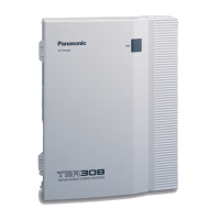
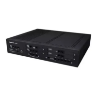
Overview of the main unit's general characteristics and capabilities.

3.2. Characterstics

Detailed technical characteristics like CPU, power, dialling, and environment.

4 Technical Descriptions

4.1. Block Diagram

High-level block diagram illustrating the system architecture and component connections.

4.3. Expansion Unit

4.4. Power Circuit

4.5. Power Supply Unit

4.5.1. Block Diagram and Circuit Description of PSU

Block diagram and circuit explanation for the Power Supply Unit.

4.6. AC input, Rectification Smoothing Circuit

4.7. Main Converter

4.8. Output voltage

2) 41V Output voltage

4.9. Battery voltage input and output

4.11. Protection Circuit

5 Location of Controls and Components

6 Installation Instructions

7 Operating Instructions

8 Test Mode

9 Troubleshooting Guide

9.1. MPR/SPR/Mother Board

Troubleshooting guide for the MPR, SPR, and Mother Board, including LED status.

9.1.1. Startup

Flowchart for diagnosing startup issues related to power, cables, and board checks.

9.1.2. Battery Alarm

9.1.3. Using Voice Mail

9.2. Power Supply

9.2.1. No Voltage is Output at All (1)

Troubleshooting flowchart for diagnosing complete lack of voltage output from the main converter.

9.2.2. No voltage is Output at All (2)

Continuation of troubleshooting for no voltage output, focusing on short circuits and 15V output.

9.2.3. 41V are Not Output

9.2.4. Battery Backup Function Does Not Operate / PSU can Not Charge Batteries

10 Disassembly and Assembly Instructions

11 Miscellaneous

11.1. How To Replace a Flat Package IC

Detailed procedure for replacing high-pin-count flat package ICs using basic tools.

11.2. How to Replace the LLP (Leadless Leadframe Package) IC and IC ground plate

11.3. Terminal Guide of the ICs, Transistors and Diodes

12 Schematic Diagram

12.1. Mother Board

Detailed schematic diagrams for various sections of the Mother Board.

12.1.2. No.2

12.1.3. No.3

12.1.4. No.4

12.1.5. No.5

12.1.6. No.6

12.1.7. No.7

12.3. CPU Board

12.3.4. No.4

12.3.5. No.5

12.3.6. No.6

12.7. Waveform

12.7.1. CPU Board Voltage

Table and visual representation of CPU board voltage specifications and ripple.

12.7.4. CPU Board NAND Access

12.7.5. CPU Board SRAM Access

12.7.6. Power Supply Board

13 Printed Circuit Board

13.5. Power Supply Board

15 Exploded View and Replacement Parts List

15.4. Replacement Parts List

15.4.4. CPU Board Parts

15.4.5. Power Supply Board parts

Related product manuals