11
KX-NS500AG
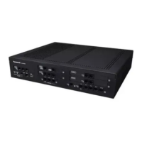
4.3. Expansion Unit
The expansion unit is constructed by CPU Board (SPR) and Mother Board. The block diagram and operation of each card are
described here.
4.3.1. CPU Board (SPR)
Fig.4 shows detail block diagram of CPU Board (SPR), and each function of CPU Board (SPR) is described in Table.6.
Table.6 CPU Board (SPR) Function Description
Card Description
CPU CPU controls the line card in the expansion unit by the control from an CPU Board (MPR).
DDR3 DDR3 is main memory of CPU Board (SPR). Operating system, application program and concerning data are
stored in this memory.
NAND Flash CPU program is stored in this memory.
FPGA FPGA provides control and monitoring function of each line card.
ARM
Cortex- A 8
300MHz
L1 32K/32K w/SED
L2256K w/ECC
176K ROM 64K RAM 64K RAM
Crypto
DDR
Interface
DDR3
128MB
NAND
NAND
FLASH
256MB
UART
SD
GPIO
Interrupt
etc.
DC/DC(+3.3V,+1.8V,+1.1V)
AC_ALM, DC_ALM, System Reset, FPGA_REBOOT, DONE
Slave
FPGA
LED
+5V
Externalbus
80PIN CONNECTOR (CPU Interface)
STATUS
DC/DC
+3.3V
+15V
8bit
8bit
+5V
+VBAT
LVDS
Down
Highway
Up
Highway
FH+CLK
(8MHz)
Interrupt
Exp I/F
RJ45
NETREF
Expansion bus
Fig.4 CPU Board (SPR) Block Diagram
 Loading...