PDP-435PE
47
5678
56
7
8
C
D
F
A
B
E
6.2 DRIVE ASSY ADJUSTMENT
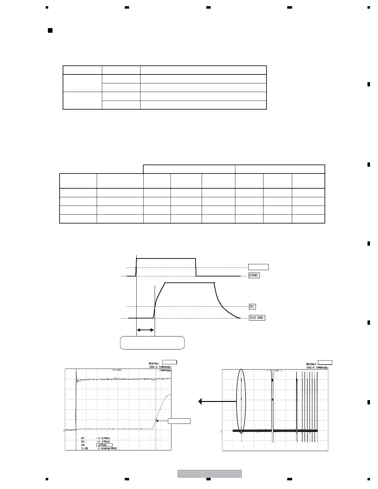
How to readjust the timing of the control signals when the DRIVE Assy TND506MD is
to be replaced
As there is a large difference in delay time among the individual TND506MDs, timing adjustment has been made on each
TND506MD in the unit process. If the TND506MD is replaced on the X or Y Drive Assy, readjustment of the timing of the
control signals is required.
• How to adjust
Adjust the timing between the startup of the control signals of SUS-U1, SUS-D1, SUS-U2, and SUS-D2 and the startup
of the voltage between the gate and the source of the output FET, with the VR resistors that are inserted in the signal
line in series. When adjusting, set the unit to Drive OFF mode, and Vsus to 0 V. (For details on how to set to Drive OFF
mode, see "7.1.6 Power on/off function for the large-signal system".)
• Specified values for adjustment and adjustment points
Note: Connect GND of the probe with DGND (DGND: X Drive Assy: K1020, Y Drive Assy: K2010) for input signal.
For outputting a signal, obtain a signal from the FET gate terminal.
For adjustment, magnify any pulse in the waveform.
VGS=5V line
Magnify.
500us/div
50ns/div
Input signal: 1V/div
Output FET VGS 5V/div
Assy Replaced IC Signal for which Readjustment is Required
X DRIVE
IC1101 XSUS-U2 & XSUS-D2
IC1102 XSUS-U1 & XSUS-D1
Y DRIVE
IC2201 YSUS-U1 & YSUS-D1
IC2202 YSUS-U2 & YSUS-D2
X DRIVE Y DRIVE
Signal Name
Set Value for
Delay Time
Input
Signal
Output
Signal
Adjustment
VR
Input
Signal
Output
Signal
Adjustment
VR
SUS-U1 375ns ± 10ns K1005 Q1108 VR1103 K2025 Q2202 VR2201
SUS-D1 375ns ± 10ns K1009 Q1112 VR1104 K2027 Q2205 VR2202
SUS-U2 375ns ± 10ns K1008 Q1103 VR1101 K2022 Q2208 VR2203
SUS-D2 375ns ± 10ns K1006 Q1105 VR1102 K2024 Q2212 VR2204
Waveform of the
control signal
(input signal)
VGS waveform
(output signal)
• Actually measured waveforms
Adjust so that the delay is
in the range of 375 ± 10 ns.
About 2.5V
 Loading...