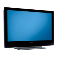
PDP-435PE
97
5678
56
7
8
C
D
F
A
B
E
Ball No. No. Pin Name Function
AA20 450 VDDLA 3.3V power supply
AA21 451 VDDLA 3.3V power supply
Y21 452 VDDL15 1.5V power supply
W21 453 VDDLA 3.3V power supply
V21 454 VDDLA 3.3V power supply
U21 455 VDDL15 1.5V power supply
T21 456 SDITCK JTAG signal
R21 457 GPIO0_4 Microcomputer macro general-purpose port
P21 458 VDD15 1.5V power supply
N21 459 YSUSA_3 Y-Drive control signal output
M21 460 YSUSA_9 Y-Drive control signal output
L21 461 VDDD15 1.5V power supply
K21 462 YSUSB_3 Y-Drive control signal output
J21 463 VBB VBB power monitor in the DRAM
H21 464 VDDD15 1.5V power supply
G21 465 YSUSB_13 Y-Drive control signal output
F21 466 SCAN_2 Scan control signal output
F20 467 VDD15 1.5V power supply
F19 468 EXA17 Flash memory address bus
F18 469 EXA2 Flash memory address bus
F17 470 EXDIO_2 Flash memory data bus
F16 471 VDD15 1.5V power supply
F15 472 EXDIO_10 Flash memory data bus
F14 473 TRNSEND_I NC pin
F13 474 VDD15 1.5V power supply
F12 475 RBI_1 B phase signal input of R video (first bit)
F11 476 VDD15 1.5V power supply
F10 477 GBI_3 B phase signal input of G video (third bit)
F9 478 BBI_7 B phase signal input of B video (seventh bit)
F8 479 BBI_1 B phase signal input of B video (first bit)
F7 480 VDD15 1.5V power supply
PDG054A (DIGITAL VIDEO ASSY : IC5401)
• PDP ASIC IC4
Pin Function (10/10)
 Loading...