PDP-506PE
86
1234
1234
C
D
F
A
B
E
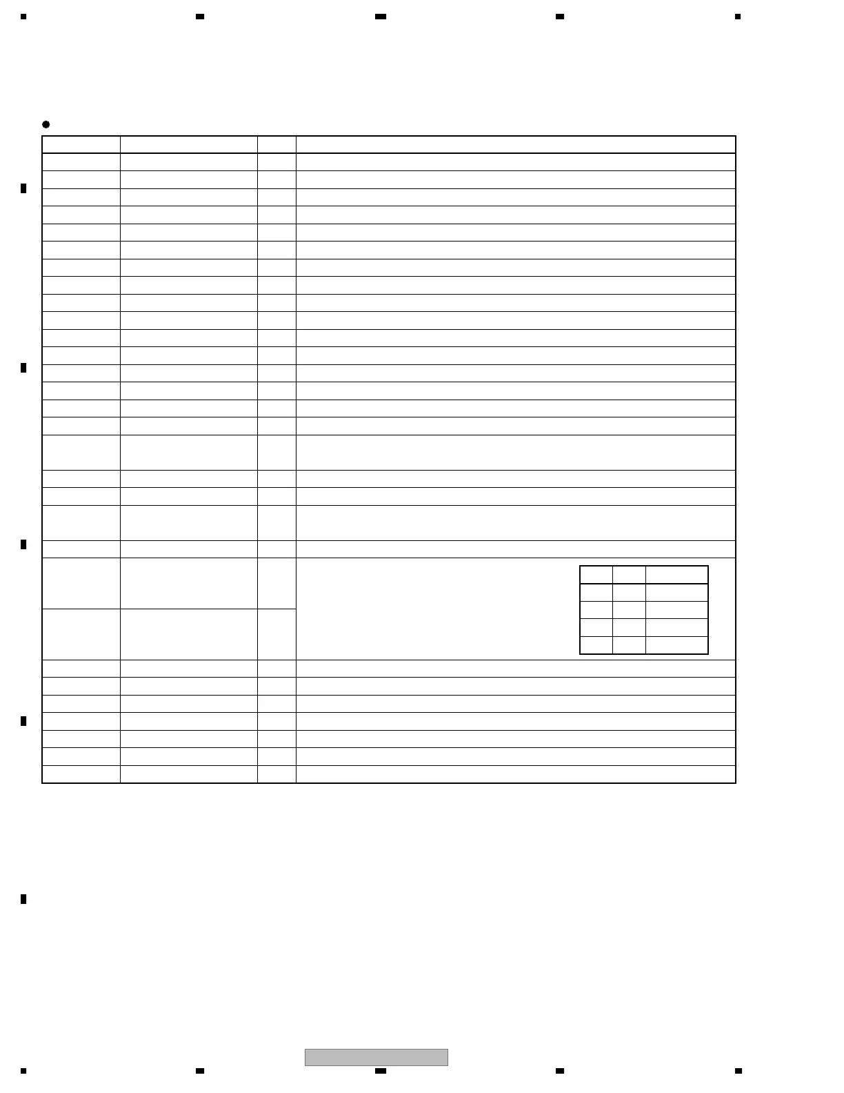
Pin Function
OC1 OC2 OUT
LLALL Hi-Z
LH DATA
HL ALL L
HH ALL H
No. Pin Name I/O Pin Function
1 - 30 OUT3 - OUT32 O High-voltage push-pull output
31 N.C. − Not connected
32 - 33 V
DDH − High-voltage circuit supply
34 N.C. − Not connected
35 - 37 GND1 − Ground
38 N.C. − Not connected
39 GND2 − Ground
40 - 41 GND1 − Ground
42 N.C. − Not connected
43 - 44 V
DDH − High-voltage circuit supply
45 N.C. − Not connected
46 - 77 OUT33 - OUT64 O High-voltage push-pull output
78 N.C. − Not connected
79 - 80 V
DDH − High-voltage circuit supply
81 N.C. − Not connected
82 - 83 GND1 − Ground
84 DIR I
Setup of shift register shift direction
L = Shift into reverse (SO → SI) H = Shift forward (SI → SO)
85 SO I/O Serial data input / output
86 CLK I Serial clock input Fetch SI or SO data to shift register by CLK rise edge
87 LAT I
LAT data input
L = Transfer shift register data to output latch H = Hold data to output latch
88 V
DD − Logic supply
89 OC1 I
Output control
Control output according to the right
truth value table
90 OC2 I
91 SI I/O Serial data input / output
92 CLR I All output reset CLR pin : L → Normal operation CLR pin : H → All output High
93 - 94 GND1 − Ground
95 N.C. − Not connected
96 - 97 V
DDH − High-voltage circuit supply
98 N.C. − Not connected
99 - 100 OUT1 - OUT2 O High-voltage push-pull output
 Loading...