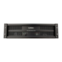
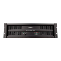
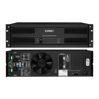
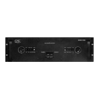
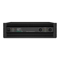
Technical Service Manual 11
ISA Series Power Amplifiers
octaves above the high end of the audio spectrum). This makes the
amplifier less susceptible to RF interference, high-frequency
oscillations, etc.
Also in this stage, the feedback loop contains one half of a 13600
dual operational transconductance amplifier (Figure 1.10). The OTA is
part of the clip limiter circuitry; when the clip limiter is activated, a
control voltage increases the transconductance of the OTA, which
essentially decreases the impedance of the feedback loop and
reduces the gain of the stage in order to reduce the amount of
clipping.
The gain control uses a linear potentiometer, but the impedances
loading the wiper to ground make the pot approximate an audio
taper over most of its rotation. After the wiper, RC networks roll
off the low end, if the LF filter is set for that channel, at either 30
or 50 Hz, depending on the DIP switch setting on the rear panel.
The next active device is another 5532 op amp, U101:2. Its output
drives the driver transistors, which in turn drive the output transis-
tors. The output section has a Class AB+B configuration; the
drivers (a complementary pair, Q105 and Q106, comprising an NPN
MJE15032 and a PNP MJE 15033) are class AB. A series network
of two diodes and a 100-ohm trimpot provide the small amount of
forward bias on the transistor pair to keep crossover distortion
minimal. In parallel with the trimpot is a 50-ohm thermistor with a
negative temperature coefficient; as the circuitry warms, its
resistance decreases. This reduces V
BE
on both Q105 and Q106,
decreasing the bias current to reduce the threat of thermal runaway.
The base of each driver transistor is tied to ground through a diode
and a 2.2K trimpot in series; these set the current limiting threshold
for their respective signal polarities.
The collector of each driver transistor directly drives the bases of
its output transistors, which are the main power-handling signal
devices. If you’re not familiar with the grounded-collector scheme,
the arrangement of the output transistors might look somewhat
R111
100
^R_0805
R109
100
^R_0805
10.0K
^R_0805
R103
3
+
8
7
5
1
4
-
2
U10:1
LM13600M
R108
7.50K
^R_0805
+14V
A1
R104
150K
^R_1206
-14V
R110
270
^R_0805
C105
100-25V
R107
^R_0805
39K
Q100
3906
R115
820
^R_1206
To input op amp U101:1
11
CLIP LIMIT
SWITCH
(Open to defeat
clip limiter)
From clip
detection
strange: the positive voltage swings are handled by PNP transis-
tors, while the negative swings are handled by NPN devices. The
collectors all connect to ground, which allows them to be mounted
directly to the heat sink—metal-to-metal, without insulators in
between—for the best possible transfer of heat away from the
transistors. The emitters of the PNP and NPN transistors are
coupled through resistors to the positive and negative supply rails,
respectively, forming banks of common-emitter circuits driving the
supply rails. Consequently, the devices drive the rails with the
audio signal, which rides atop the DC. The output to the speaker
load is taken from the point between the positive and negative
reservoir capacitors; this is also where the negative feedback is
taken from. The nature of this arrangement, with audio signal
riding on the supply rails, is why the power supply has no ground
reference.
Another unusual characteristic of the grounded-collector output
section is that the signal at the output to the speaker is actually
opposite in polarity to the signal at the op amp output. This is why
the negative feedback resistor, R122, connects to the op amp’s
non-inverting input instead of the inverting input.
The output point of the circuit couples to the output connector
through an RLC network (R160, R161, R162, L100, and C124) that
serves as a high-frequency snubber and also helps keep the amp
circuitry stable when driving capacitive loads.
Clip detection
The output of the op amp also drives a group of four diodes (D102,
D103, D105, and D106) arranged as a full-wave rectifier. Normally,
the op amp’s output signal level is about 1 volt or less, which is all
it takes to drive the driver transistors.
But because this point is within the overall feedback loop, when
clipping occurs, the op amp puts out a much higher signal voltage
to try to make the output signal track the input. The four diodes
rectify the voltage to drive the clip indicator LED, LD100. The
current exiting the full-wave rectifier passes to ground through
R127 and also drives the base of transistor Q100 through R115. If
the clip limiter is switched on, Q100’s emitter is grounded, and
when the voltage across R127 goes sufficiently negative to
forward-bias Q100, which sends current through R111 and R103
into the amplifier bias input of the operational transconductance
amplifier (OTA), U10:1. The OTA is in the negative feedback loop of
U101:1, and increasing its transconductance essentially reduces
the impedance of the feedback loop, which reduces the gain of the
op amp stage. This reduces the signal level until the amount of
clipping is minimal. When the clipping stops, Q100 is no longer
forward-biased, and the gain returns to normal.
DC protection
The ISA750 and ISA800T have a crowbar circuit, based on a triac
and two silicon controlled rectifiers, on each output to protect
against DC faults. If an amp channel puts out a DC voltage, which
could be the result of a component or circuit failure, it will first
trigger either D119 or D120, depending on the polarity of the
Figure 1.10