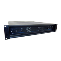
Technical Service Manual 13
ISA Series Power Amplifiers
From amplifier
output circuitry
25V
70V
100V
8, 4, or 2
1.7 ISA1350 circuitry
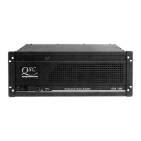
Compared to the utter simplicity of the lower power ISA models
like the ISA280, the ISA1350’s circuitry might seem so complex
that it should belong to another family of power amps. This added
complexity primarily concerns two particular areas of the ampli-
fier—the class H power supply rail steps and the bias circuitry—
and provides these benefits:
• Three-tier class H output section—the additional tier
further exploits the dynamic nature of audio to improve the
amplifier’s electrical efficiency to as much as 55% better than a
class AB amplifier of a comparable power rating. Despite the
added circuitry and complexity, this allows substantial savings
in components and materials costs by scaling down power
transformers, using fewer output devices, and removing less
waste heat.
• Improved thermal bias tracking and better fault protec-
tion muting—instead of using a simple bias network based on
a series diode pair, the ISA1350 features an “active” bias
network that uses current sources to set bias. An NTC ther-
mistor mounted to the heat sink tracks the operating tempera-
ture of the output devices and directs the current sources to
compensate for optimal bias; the thermal tracking circuitry is
thus isolated from the audio signal, so it can perform with
great precision. The protection circuits for faults, overcurrent,
etc., are also tied into the bias network, so they can shut off
the bias if a serious problem occurs. Shutting off the bias then
shuts off current in the output transistors. This is a highly
effective and inherently balanced approach to fault protection,
which is especially important in a very high power amplifier.
This is also how the turn-on and turn-off muting is handled.
Class H step drivers
The step driver circuitry in the ISA1350’s three-tier class H system
is very similar to the one used in the two-tier system of the ISA750
and ISA800Ti. Since the normal voltage limit for 1206-type
surface-mount resistors is 200 volts and the voltages that the step
driver’s voltage sensing resistors see may reach 300 volts, the
ISA1350 uses 100 kΩ 1206 resistors in series pairs instead of
single 200 kΩ components.
Bias circuitry
The new circuitry (see Figure 1.13) for the bias network features
transistors Q108 and Q109, with surrounding resistors, forming 8
mA current sources, with less loading of the op amp output than
the resistors used on older RMX and ISA models. These currents
forward bias diodes D106 and D107, which are in contact with the
heat sink. Trimmer R171 adjusts the bias voltage.
The bias currents are controlled by signals +BIAS and –BIAS,
which come from a current source Q142, Q143, and R250. The
single voltage across R250 determines the voltage across both
R161 and R166, which sets the bias currents equally for the PNP
and NPN drivers.
The voltage on R250 is controlled by the voltage at the collector of
Q132, which forms a Vbe multiplier controlled by R226 and R227.
The collector voltage is a multiple of the base voltage, with a
nominal value of 5.45 times the base voltage. A typical 25°C base
voltage is 0.68 V, resulting in a collector voltage of 4.4 V. The
current thru R233 subtracts about 1 V from this, and stabilizes the
voltage against changes in supply voltage. As the amplifier heats
up, the base voltage declines somewhat, and therefore, the BIAS
signals are reduced, which adds more thermal compensation.
The thermal sensor R239 is a 10 kΩ NTC resistor (not a PTC as
used in the other models); its resistance decreases with rising
temperature. This increases voltage across R240, and thus reduces
voltage between Q142 and Q143, which reduces bias currents. The
voltage on R240 ranges from almost zero when cold, to about 0.6 V
at maximum temperature.
Muting via the bias network
Muting occurs when the emitter current for Q141 is removed, thus
shutting down Q142 and Q143 and removing all bias from the
output section. The emitter current for Q141, through R238, is
controlled by the voltage on C131.
• When the amp is turned on, C131 ramps up from zero, using a
small current from R220. When the voltage on C131 exceeds
the voltage on the collector of Q132 (the bias reference
voltage), Q141 is turned on, and the bias circuit is enabled.
• When the amp is turned off, circuitry on the AC board pulls
down on D119 and quickly discharges C131, thus muting the
amplifier.
• When the amplifier reaches full temperature, circuitry on the
AC board senses the voltage on the FAN-SP line, from D122,
and triggers the discharge circuit for D119, thus muting the
amplifier.
Figure 1.12