M10 Hardware Design
M10_HD_V3.0 - 17 -
1) When the module works in this temperature range, the deviation from the GSM
specification might occur. For example, the frequency error or the phase error could
increase.
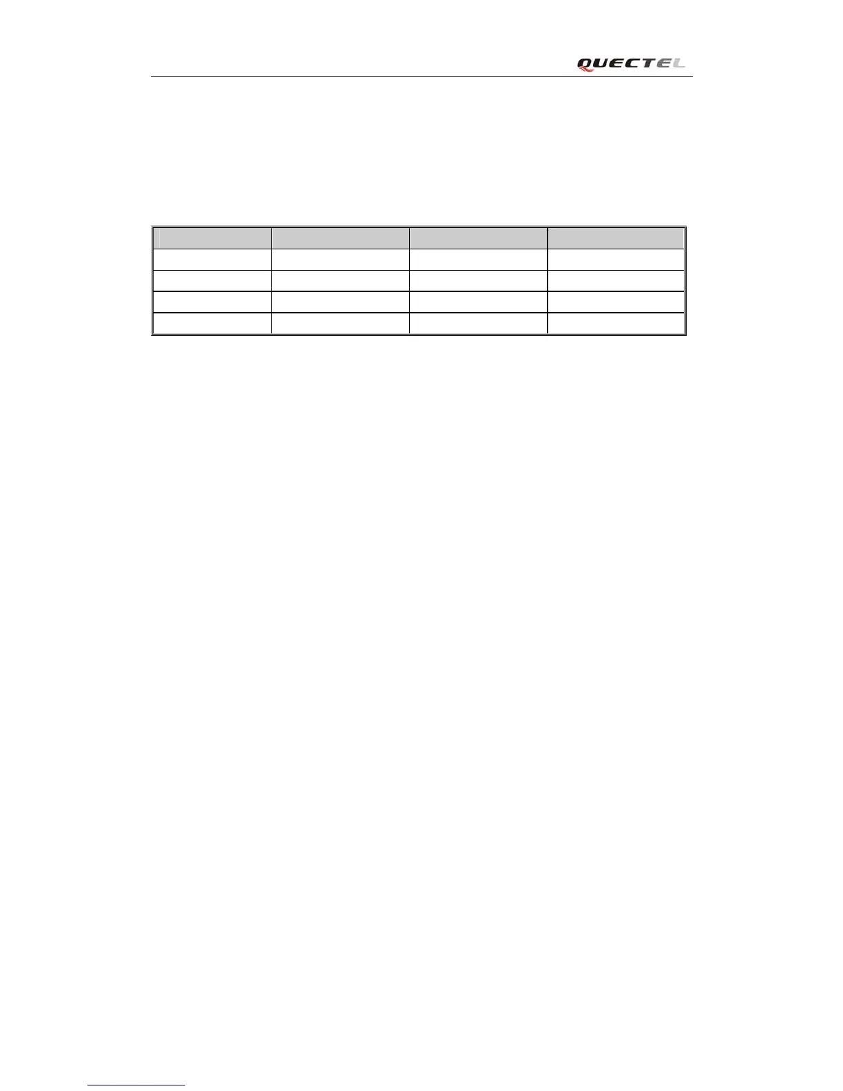
Table 4: Coding schemes and maximum net data rates over air interface
Coding scheme 1 Timeslot 2 Timeslot 4 Timeslot
CS-1: 9.05kbps 18.1kbps 36.2kbps
CS-2: 13.4kbps 26.8kbps 53.6kbps
CS-3: 15.6kbps 31.2kbps 62.4kbps
CS-4: 21.4kbps 42.8kbps 85.6kbps
2.2. Functional diagram
The following figure shows a block diagram of M10 and illustrates the major functional parts.
Power management
Baseband
Serial Flash
The GSM radio frequency part
The Peripheral interface
—Power supply
—Turn on/off interface
—UART interface
—Audio interface
—SIM interface
—Keypad interface
—ADC
—SD card interface
—RF interface