M10 Hardware Design
M10_HD_V3.0 - 57 -
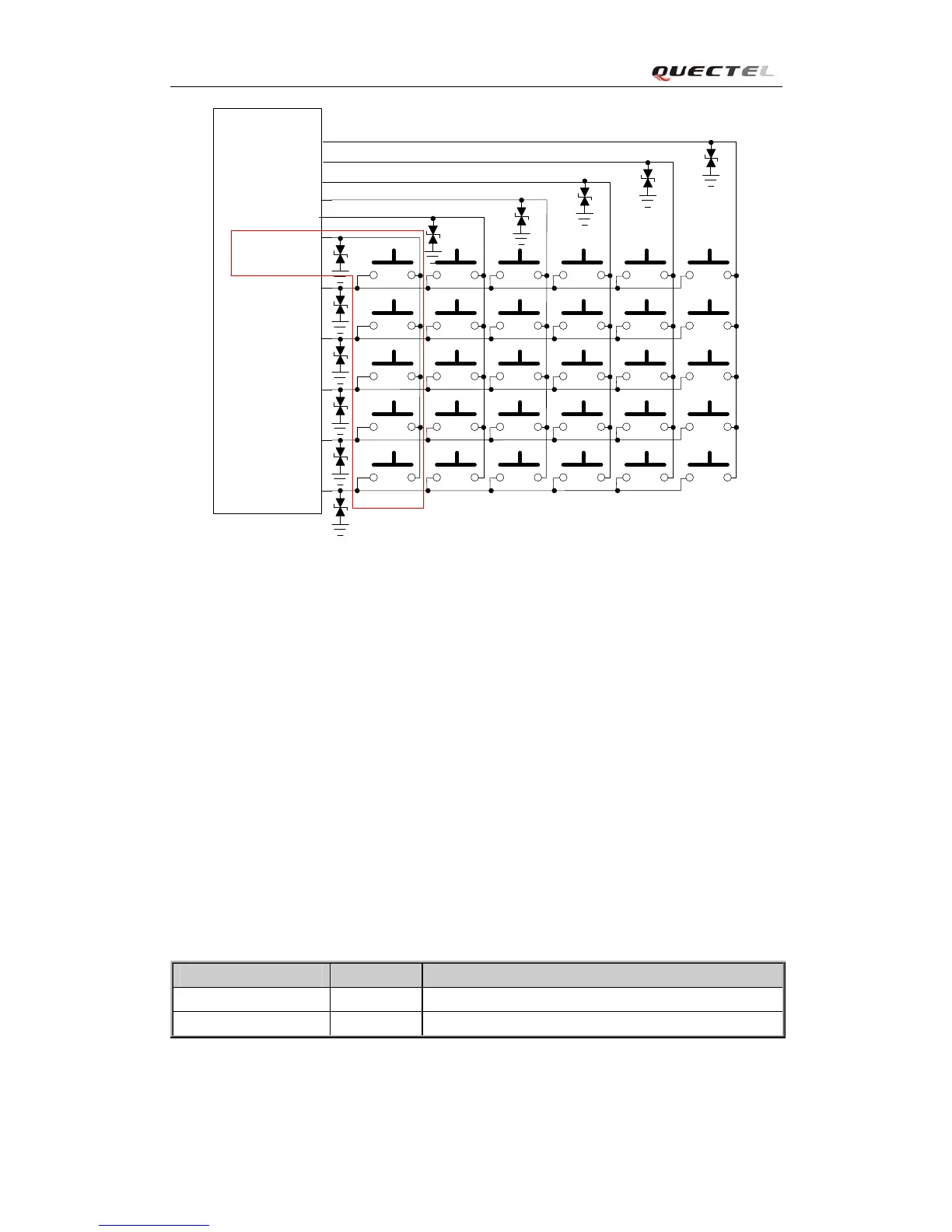
KBR4
KBR3
KBR2
KBR1
KBR0
KBC0
KBC1
KBC2
KBC3
KBC4
Module
GPIO1_KBC5
Figure 37: Reference circuit of the keypad interface
If a 5*5 matrix does not provide enough keys, GPIO1 could be multiplexed as KBC5 to configure
a 5*6 keypad matrix. Then, the keypad interface consists of 5 keypad row outputs and 6 keypad
column inputs. The basic configuration is 5 keypad rows and 6 keypad columns, giving 30 keys.
Note: This function is not supported in the default firmware.
3.12. ADC
The module provides two auxiliary ADC interfaces to measure the values of two analog inputs.
AT command “AT+QADC?” is used to read the voltage value present on ADC0 pin. AT
command “AT+QEADC?” is used to read the voltage value present on ADC1 pin. For details of
this AT command, please refer to
document [1].
Table 18: Pin definition of the ADC
Name Pin Function
ADC0 41 Analog to digital converter.
ADC1 40 Analog to digital converter