M10 Hardware Design
M10_HD_V3.0 - 22 -
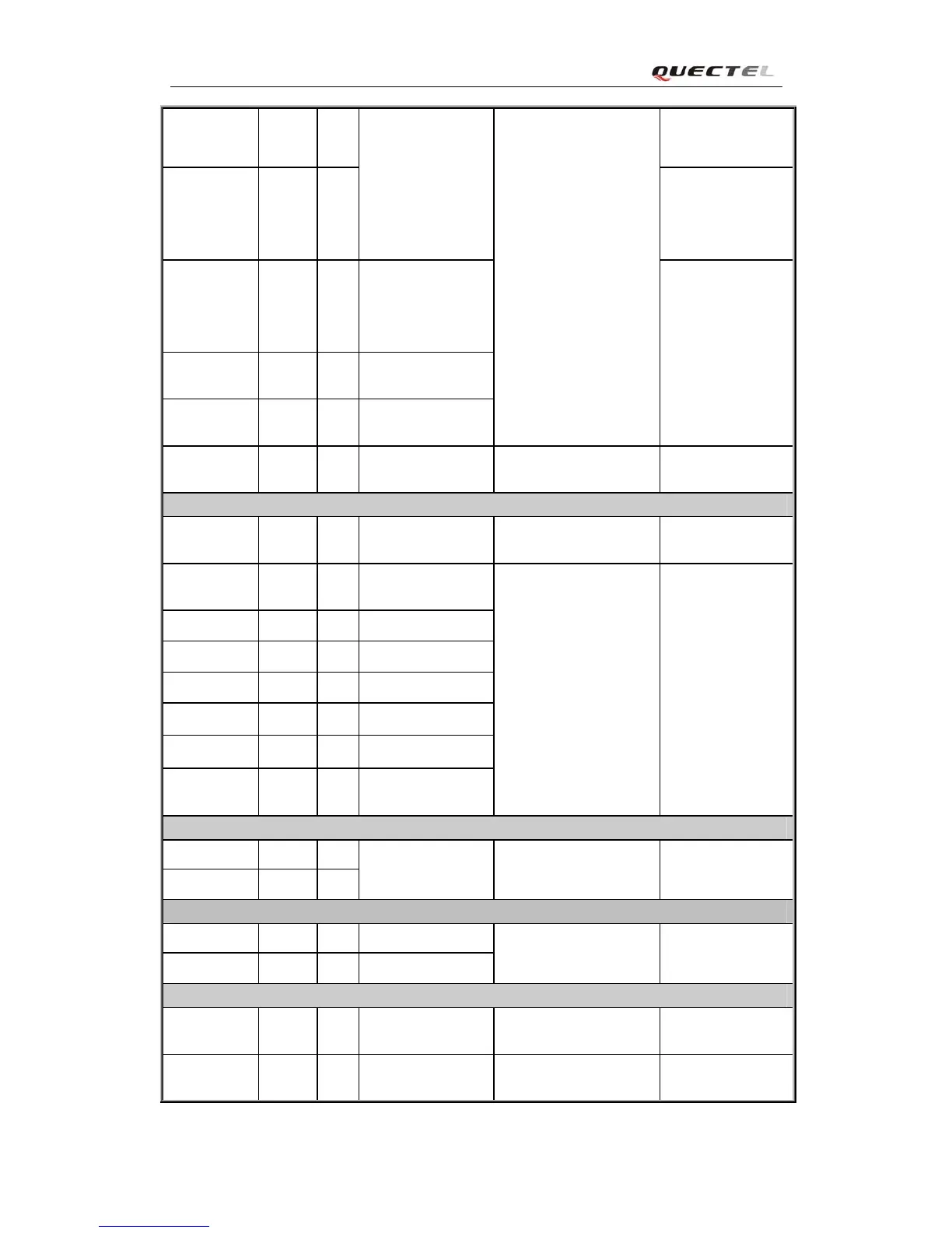
KBC0~
KBC4
33~37
I Keypad interface VILmin=-0.3V
VILmax=
0.25*VDD_EXT
VIHmin=
0.75*VDD_EXT
VIHmax=
VDD_EXT+0.3
VOLmax=
0.15*VDD_EXT
VOHmin=
0.85*VDD_EXT
If unused, keep
these pins open.
KBR0~
KBR4
28~32
O Pull up to
VDD_EXT, if
unused, keep these
pins open.
GPIO1_
KBC5
38
I/O Normal
input/output
port/Keypad
interface
If unused, keep
these pins open.
GPIO0 64 I/O Normal
input/output port
NETLIGHT 6 O Network status
indication
LIGHT_
MOS
27
O Open drain output
port
Imax=60mA If unused, keep
this pin open.
Main Serial port
PIN NAME PIN
NO.
I/O DESCRIPTION DC
CHARACTERISTICS
COMMENT
DTR 59 I Data terminal
ready
VILmin=-0.3V
VILmax=
0.25*VDD_EXT
VIHmin=
0.75*VDD_EXT
VIHmax=
VDD_EXT+0.3
VOLmax=
0.15*VDD_EXT
VOHmin=
0.85*VDD_EXT
If only use TXD,
RXD and GND to
communicate,
recommend
connecting RTS to
GND via 0R
resistor and
keeping other pins
open.
RXD 61 I Receive data
TXD 60 O Transmit data
RTS 58 I Request to send
CTS 57 O Clear to send
RI 55 O Ring indicator
DCD 56 O Data carrier
detection
Debug port
DBG_TXD 10 O Serial interface for
debugging only
Same as above If unused, keep
these pins open.
DBG_RXD 9 I
UART3
TXD3 62 O Transmit data Same as above If unused, keep
these pins open.
RXD3 63 I Receive data
SD card interface
PIN NAME PIN
NO.
I/O DESCRIPTION DC
CHARACTERISTICS
COMMENT
SD_DATA 1 I/O SD serial data VILmin=-0.3V If unused, keep