5G Module Series
RG255C-GL_Mini_PCIe_Hardware_Design 21 / 57
3.4. Power Supply
The following table shows the definition of VCC_3V3 pins and GND pins.
Table 7: Definition of VCC_3V3 and GND Pins
The typical supply voltage of RG255C-GL Mini PCIe is 3.3 V. The power supply must be able to provide a
rated output current of 3.5 A at least, and a bypass capacitor of not less than 470 µF with low ESR should
be used to prevent the voltage from dropping. If a switching power supply is used to power the module,
the power device and the routing traces of the switching power supply should avoid the antennas as much
as possible to prevent EMI interference.
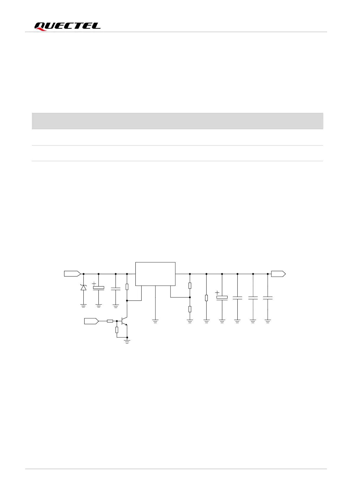
The following figure shows a reference design of power supply where R2 and R3 are 1% tolerance
resistors and C3 is a low ESR capacitor.
4, 9, 15, 18, 21, 26, 27, 29, 34, 35, 37, 40, 43, 50