5G Module Series
RG255C-GL_Mini_PCIe_Hardware_Design 26 / 57
Table 10: Pin Definition of Main UART
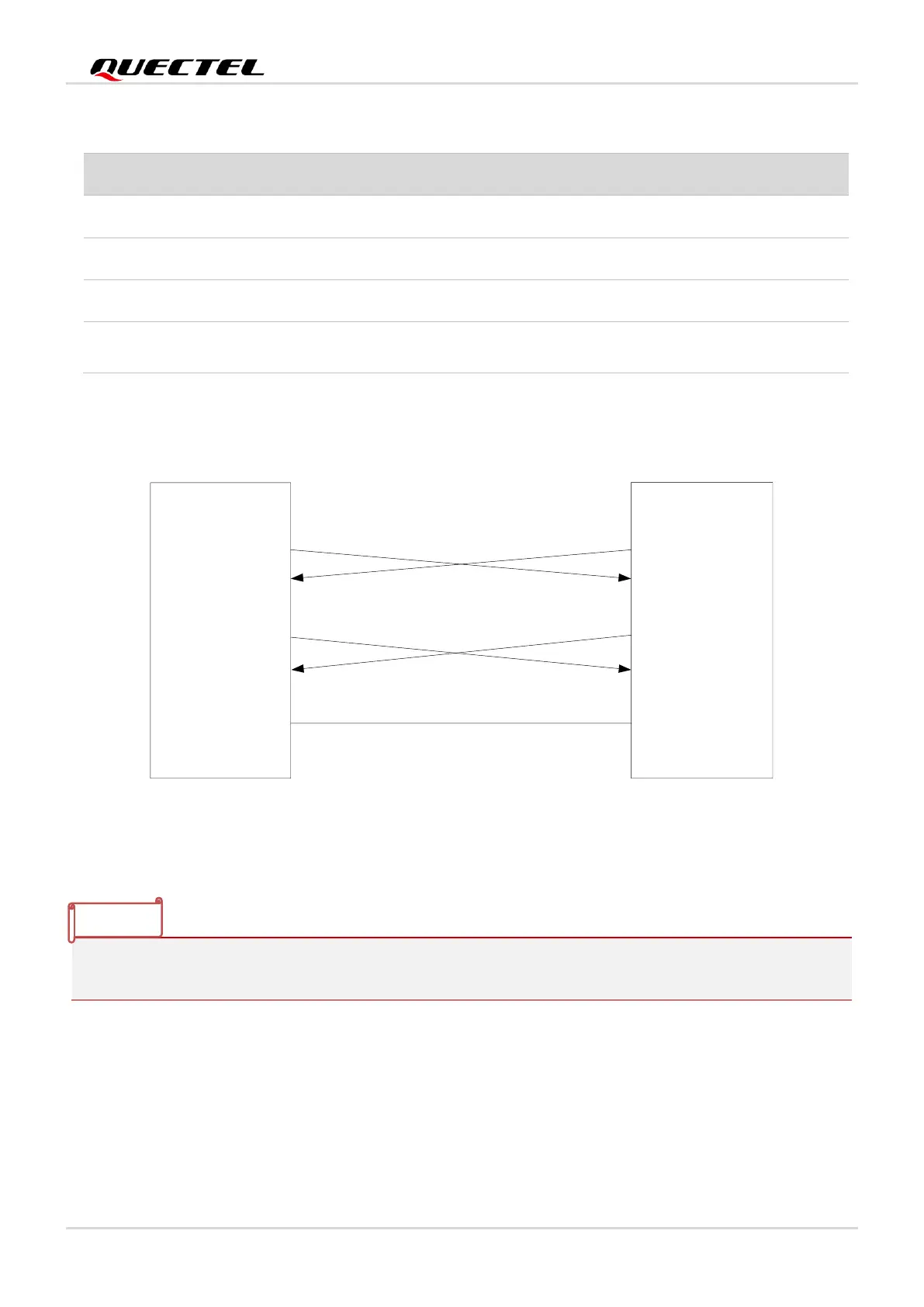
The signal level of main UART is 3.3 V. When connecting to MCU, you need to pay attention to the signal
direction. The reference circuit is shown as below:
MCU
TXD
RXD
RXD
TXD
RTS
CTS
RTS
CTS
GND
Module
GND
Voltage level: 3.3 V
Voltage level: 3.3 V
Figure 8: Reference Circuit of Power Supply
⚫
AT+IPR can be used to set the baud rate of the main UART, and AT+IFC can be used to set the hardware
flow control (hardware flow control is disabled by default). See document [3] for details.
4.4. PCM* and I2C Interfaces
RG255C-GL Mini PCIe provides one Pulse Code Modulation (PCM) digital interface and one I2C
interface.
Clear to send signal to the module
Request to send signal from the
module