5G Module Series
RG255C-GL_Mini_PCIe_Hardware_Design 27 / 57
The following table shows the pin definition of PCM and I2C interfaces that can be applied in audio codec
design.
Table 11: Pin Definition of PCM and I2C Interfaces
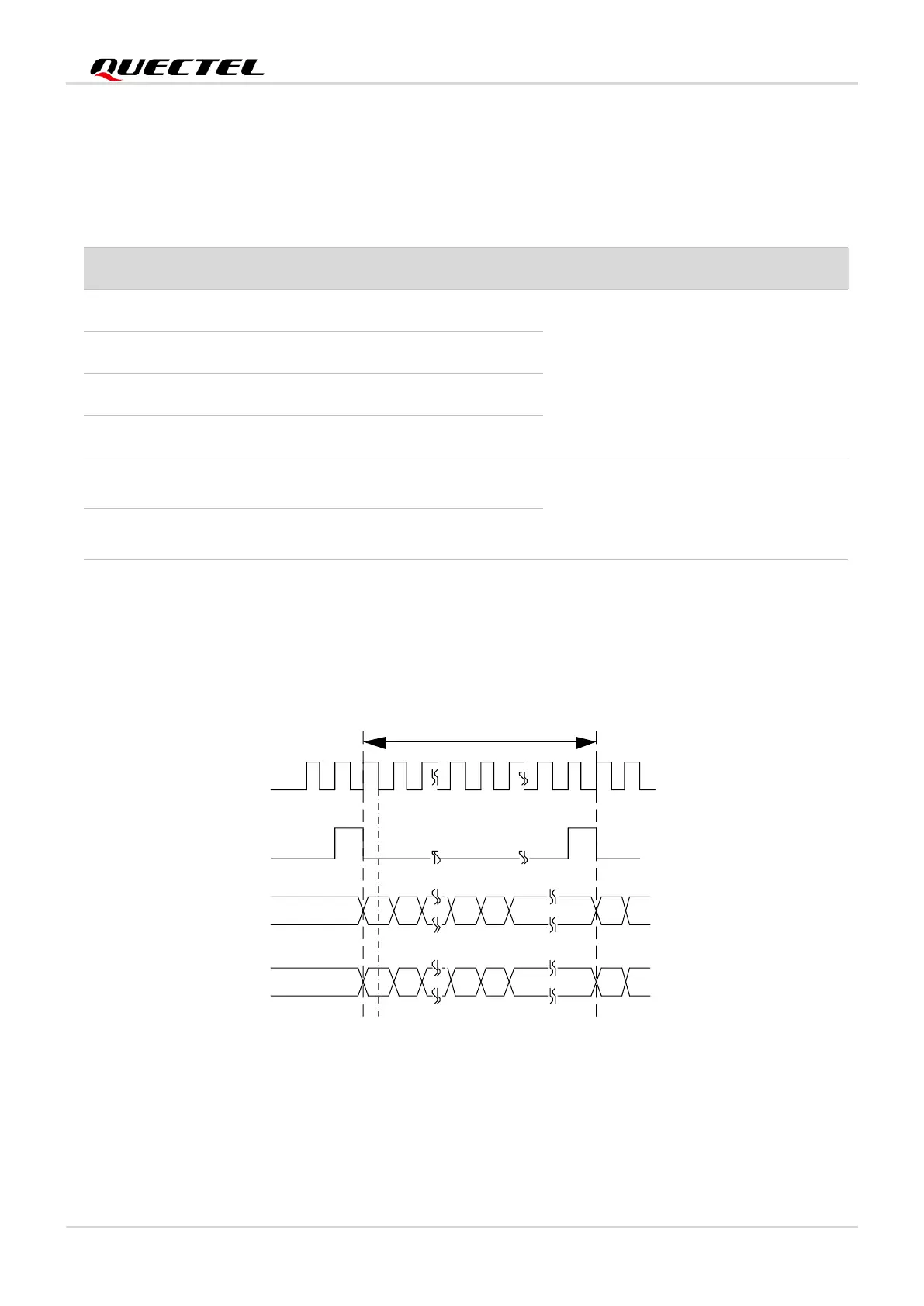
In primary mode, data is sampled on the falling edge of PCM_CLK and transmitted on the rising edge.
The PCM_SYNC falling edge represents the MSB. In this mode, PCM_CLK supports 256 kHz, 512 kHz,
1024 kHz and 2048 kHz when PCM_SYNC operates at 8 kHz, and also supports 4096 kHz when
PCM_SYNC operates at 16 kHz.
Figure 9: Timing in Primary Mode
In auxiliary mode, data is also sampled on the falling edge of the PCM_CLK and transmitted on the rising
edge. But in this mode, the PCM_SYNC rising edge represents the MSB. PCM_CLK supports 256 kHz,
512 kHz, 1024 kHz and 2048 kHz when PCM_SYNC reaches 8 kHz with a 50 % duty cycle.