EasyManua.ls Logo

Quectel RM520N-GL - Reference Design for Power Supply

Quectel RM520N-GL
88 pages
To Next Page IconTo Next Page
To Previous Page IconTo Previous Page
Loading...
5G Module Series
RM520N-GL_Hardware_Design 31 / 84
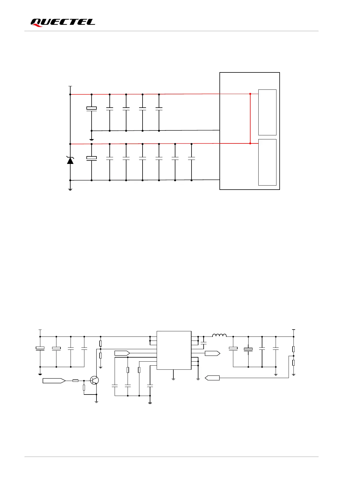
In addition, to guarantee stability of the power supply, it is recommended to use a TVS with working peak
reverse voltage of 5 V.
Module
PMU
2, 4
C2
220 μF
3, 5, 11
VCC (3.7 V Typ.)
VCC
GND
C10
68 pF
C8
220 pF
C6
6.8 nF
C4
100nF
+
C1
220 μF
TVS
VCC
GND
C9
15 pF
C7
68 pF
C5
220pF
C3
100nF
+
27, 33, 39,
45, 51, 57,
71, 73
70, 72, 74
APT
C12
4.7 pF
C11
9.1 pF
Figure 6: Reference Circuit for VCC
3.3.2. Reference Design for Power Supply
Power design is critical as the module’s performance largely depends on its power source. If the voltage
difference between the input and output is not too big, it is suggested that an LDO is used when supplying
power for the module. If there is a big voltage difference between the input source and the desired output
(VCC = 3.7 V Typ.), a buck DC-DC converter is preferred.
The following figure shows a reference design for +5.0 V input power source based on a DC-DC
converter. The typical output of the power supply is about 3.7 V and the maximum load current is 3.0 A.
PWR_IN
C8
100 μF
C10
100nF
C9
100 uF
+
R1
88.7k
U1
Q1
NPN
R8
47k
R7
4.7k
PWR_EN
R4
182k
PWR_OUT
L1
1.5 μH
VIN
VIN
VIN
EN
VSNS
COMP
RT/CLK
SS
PH
PH
PH
BOOT
PWRGD
GND
GND
AGND
VFB
R5
330k 1%
R6
100k 1%
C6
100 nF
PWRGD
EP
R2
35.7k
C7
10 nF
R3
10k
C6
10 nF
VFB
C3
100 nF
C4
33 pF
C1
220 μF
+
+
C2
220 μF
C5
NM_0.5pf
+
C11
33pF
Figure 7: Reference Circuit for Power Supply

Table of Contents