5G Module Series
RM520N-GL_Hardware_Design 35 / 84
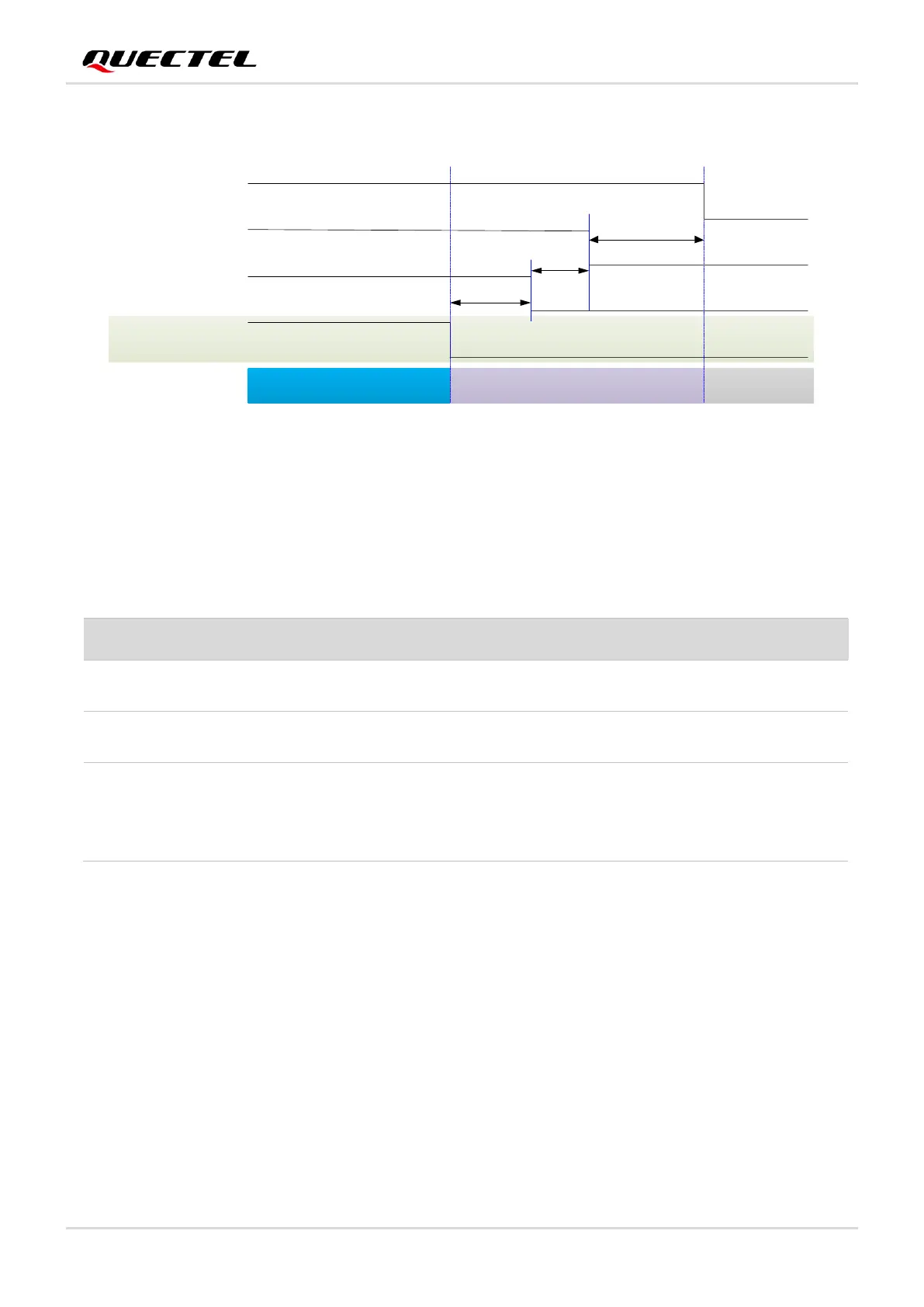
The timing of turning-off scenario is illustrated by the following figure.
VCC(H)
FULL_CARD_
POWER_OFF#
Module Status
RESET#
V
IL
≤
0.7 V
Running OFF
1.8 V
3.7 V
V
IH
≥ 1.19 V
T
FCPO#
NOTE:
When the module is in USB mode, please ignore the PCIe related signals and their timing parameters in the figure.
Active Turn-off procedure OFF
PCIE_RST_N
T
PERST#-RESET#
T
RESET#-FCPO#
Execute AT+CFUN=0,
and the module responds OK
Figure 10: Turn-off Timing through FULL_CARD_POWER_OFF#
Table 10: Turn-off Timing of the Module through FULL_CARD_POWER_OFF#
3.6. Reset
RESET# is an active LOW signal (1.8 V logic level). When this pin is active, the module will immediately
enter reset condition.
Please note that triggering the RESET# signal will lead to loss of all data in the module and removal of
system drivers. It will also disconnect the modem from the network.
Time from host pulling down PCIE_RST_N to
pulling down RESET#
Time from host pulling down RESET# to
pulling down FULL_CARD_POWER_OFF#
Time from the host pulling down the
FULL_CARD_POWER_OFF# to the module
shutdown. Ensure that the module has been
powered off completely