5G Module Series
RM520N-GL_Hardware_Design 48 / 84
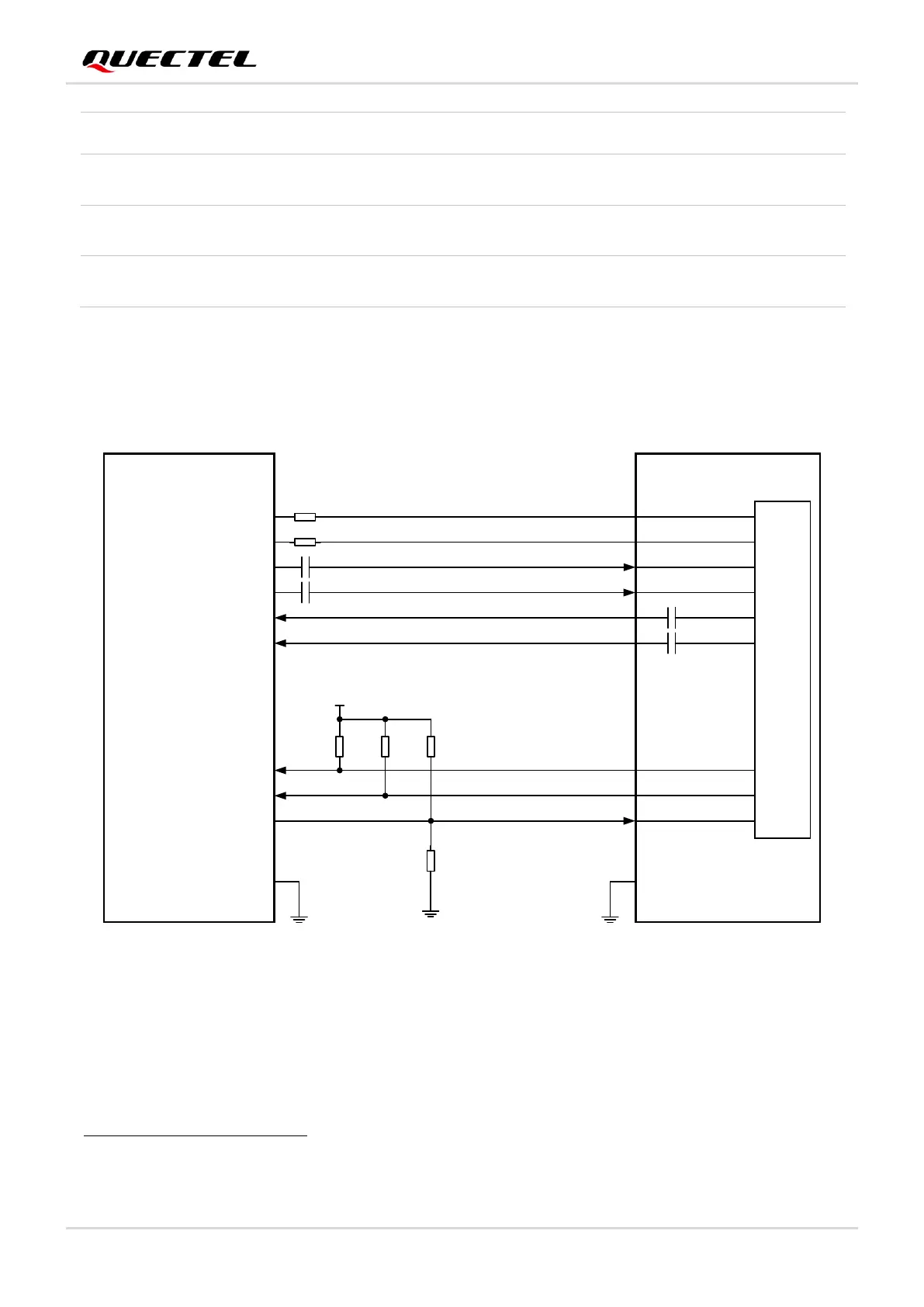
4.3.3. Reference Design for PCIe
The following figure shows a reference circuit for the PCIe interface.
Host Module
PCIE_REFCLK_P
PCIE_REFCLK_M
PCIE_RX_P
PCIE_RX_M
PCIE_TX_P
PCIE_TX_M
BB
PCIE_REFCLK_P
PCIE_REFCLK_M
PCIE_RX_P
PCIE_RX_M
PCIE_TX_P
PCIE_TX_M
55
53
49
47
43
41
PCIE_CLKREQ_N
PCIE_RST_N
PCIE_WAKE_N
PCIE_CLKREQ_N
PCIE_RST_N
PCIE_WAKE_N
VCC_IO_HOST
54
52
50
NOTE: The voltage level VCC_IO_HOST of these three signals depend on the host side due to open drain.
R5 0 Ω
R4 0 Ω
C3 220 nF
C4 220 nF
C1 220 nF
C2 220 nF
R1
10k
R2
10k
R3
4.7k
R4
NM_10k
Figure 20: PCIe Interface Reference Circuit
To ensure the signal integrity of PCIe interface, AC coupling capacitors C3 and C4 should be placed close
to the host on PCB. C1 and C2 have been integrated inside the module, so do not place these two
PCIE_RST_N behaves as DI in PCIe EP mode, and as OD in PCIe RC mode. PCIE_CLKREQ_N and PCIE_WAKE_N
behave as OD in PCIe EP mode, and as DI in PCIe RC mode. PCIe EP mode is configured by default.
PCIe clock request
Active LOW