RZ/A2M SUB Board RTK79210XXB00000BE 2. Function specifications
R20UT4398EJ0100 Rev.1.00 2-27
2018.10.11
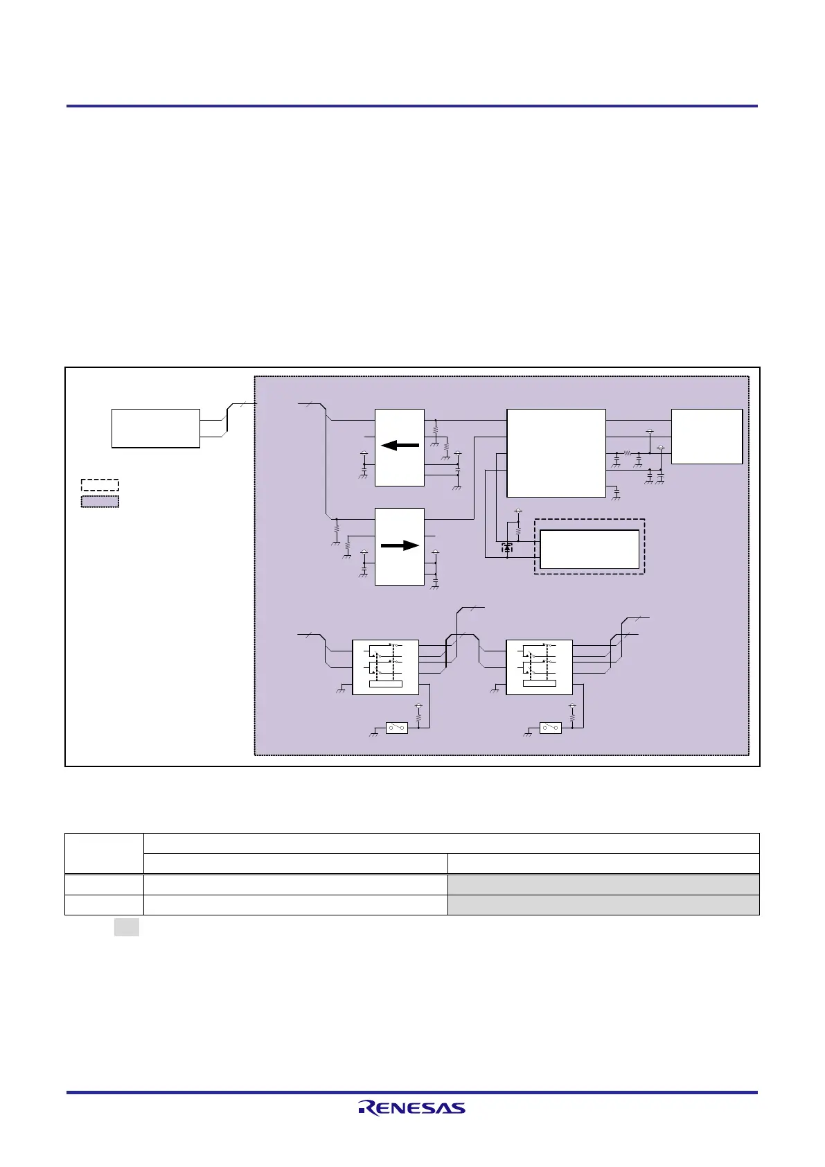
2.5 Serial Interface
On the RTK79210XXB00000BE, channel 4 of serial communications interface built into the RZ/A2M on-chip FIFO
(SCIFA) is connected to the serial port connector (USB Micro-B) (CN5) via the USB serial converter IC (RL78/G1C).
When equipping and connecting E1 connector (J1), be sure of the direction of the number 1 pin.
Figure 2.5.1 shows the serial interface block diagram, and Table 2.5.1 shows the function setting table of DIP switches
SW6-1 and SW6-3 for system setting.
For performing serial communication between the USB connector of the host computer and the serial port connector
(CN5) of RTK79210XXB00000BE, the driver of USB serial converter IC must be installed to the host computer.
Download and install the inf file onto the host computer from the following URL.
URL:TBD
Figure 2.5.1 Serial Interface Block Diagram
Table 2.5.1 Function Setting Table of DIP Switches SW6-1 and SW6-3 for System Setting
2
P9_0
P9_1
RZ/A2M (U1)
P9_1 / A9 / DRP15 / RxD4
P9_0 / A8 / DRP16 / TxD4
SDRAM / Other(UART)
(U8)
P9_1
P9_0
P9_1
P9_0
MUXOE# S
2A
2B1
2B2
1A
1B1
1B2
2
DRP /
Other(UART)(U11)
RxD4
TxD4
P9_1
P9_0
MUX
OE# S
2A
2B1
2B2
1A
1B1
1B2
2
To SDRAM
2
To DRP I/F
3.3V
DIP
SW6-1
OFF
3.3V
DIP
SW6-3
OFF
VBUS
D+
D-
USB Micro-B
Receptacle (CN5)
5V
RL78/G1C(U23)
P51 / TxD0
P50 / RxD0
RESET#
UDP0
UDM0
UVBUSP40 / TOOL0
VDD
UVDD
E1 connector(J1)
TOOL0
RESET#
【A】
2
【B】
2 2
【A】 【B】
3V5V
Level shifter (U22)
5V
VCCB
3.3V
VCCA
RxD4
A0
A1
B0
B1
3V5V
Level shifter (U25)
5V
VCCB
3.3V
VCCA
TxD4
A0
A1
B0
B1
DIR
DIR
5V
NC
NC
5V
Note: Red text indicates a function used.
:Indicates a function not implemented.
:Indicates a SUB board.
ON(L):A=B1, OFF(H):A=B2 ON(L):A=B1, OFF(H):A=B2
+
 Loading...


