RZ/A2M SUB Board RTK79210XXB00000BE 2. Function specifications
R20UT4398EJ0100 Rev.1.00 2-40
2018.10.11
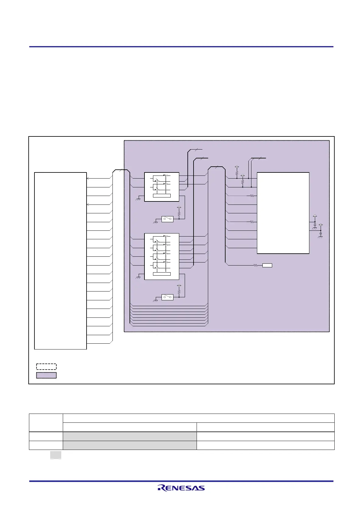
2.15 VDC6 Interface
RZ/A2M has a digital image signal input pin (DV pin) which supports YCbCr422, YCbCr444, RGB888, RGB666, and
RGB565 images. In addition, there is a digital image signal output pin (LCD pin) which supports a maximum image size
of 1999 pixels (horizontal) by 2035 lines (vertical). On the RTK79210XXB00000BE, there is a 50 pin MIL connector to
connect the DV pins and LCD pins of RZ/A2M.
Figure 2.15.1 shows the VDC6 interface block diagram, and Table 2.15.1 shows the function setting table of DIP
switches SW6-6 and SW6-7 for system setting.
Figure 2.15.1 VDC6 Interface Block Diagram
Table 2.15.1 Function Setting Table of DIP Switches SW6-6 and SW6-7 for System Setting
D[23:0]
RZ/A2M (U1)
PH_2 / DV0_DATA22 /
LCD0_DATA1
35
D1
D0
TCON[4:3]
TCON0 TCON[4:3, 0]
LCDCLK
PF_7 / DV0_DATA23 /
LCD0_DATA0
PJ_6 / FCE / LCD0_CLK
PJ_7 / NAF0 / LCD0_EXTCLK
PC_[3:4] / LCD0_TCON[4:3]
P7_7 / DV0_HSYNC /
LCD0_TCON0
PB_[5:0] / DV0_DATA[0:5] /
LCD0_DATA[23:18]
PA_7 / DV0_DATA6 /
LCD0_DATA17
P8_0 / DV0_DATA14 /
LCD0_DATA9
PF_[0:6] / DV0_DATA[15:21] /
LCD0_DATA[8:2]
PA_[3:0] / DV0_DATA[10:13] /
LCD0_DATA[13:10]
PA_6 / DV0_DATA7 /
LCD0_DATA16
PA_5 / DV0_DATA8 /
LCD0_DATA15
PA_4 / DV0_DATA9 /
LCD0_DATA14
DVCLK
D[23:18]
PA_7
PA_6
PA_5
PA_4
D[13:10]
D9
D[8:2]
VDC6 / NAND(U15)
PJ_6
PJ_7
LCDCLK
EXTCLK
35
2
To NAND flash memory
PJ_7
PJ_6
VDC6 / Other(U20)
D14
D15
D16
D17
4
PA_4
PA_5
PA_6
PA_7
P7_2 / DV0_CLK
EXTCLK
CLK
Socket(X5)
TCON[4:3, 0]
D[23:18, 13:0]
DVCLK
3.3V
DIP
SW6-6
ON
3.3V
DIP
SW6-7
ON
MUXOE# S
4A
4B1
4B2
3A
3B1
3B2
2A
2B1
2B2
1A
1B1
1B2
MUXOE# S
2A
2B1
2B2
1A
1B1
1B2
SCL3
SDA3
PD_6 / RIIC3SCL
PD_7 / RIIC3SDA
SCL3
SDA3
2
To EEPROM, CEU I/F
VDC6 connector (CN15)
(RSK+RZA1H LCD I/F)
3.3V
5V
SCL3
SDA3
PWM
INT
LCD0TCON[4:3, 0]
LCD0CLK
LCD0DATA[23:0]
SCL0
SDA0
PWM
INT
PWM
INT
P5_7 / IRQ3
INT
PWM
P7_6 / DV0_VSYNC / GTIOC3A
RES#
RES#
RES#
RES#
RES#
DVCLK
DV0CLK
3.3V
3.3V
Note: Red text indicates a function used .
:Indicates a function not implemented .
:Indicates a SUB board.
ON(L):A=B1, OFF(H):A=B2
NC
40MHz
 Loading...


