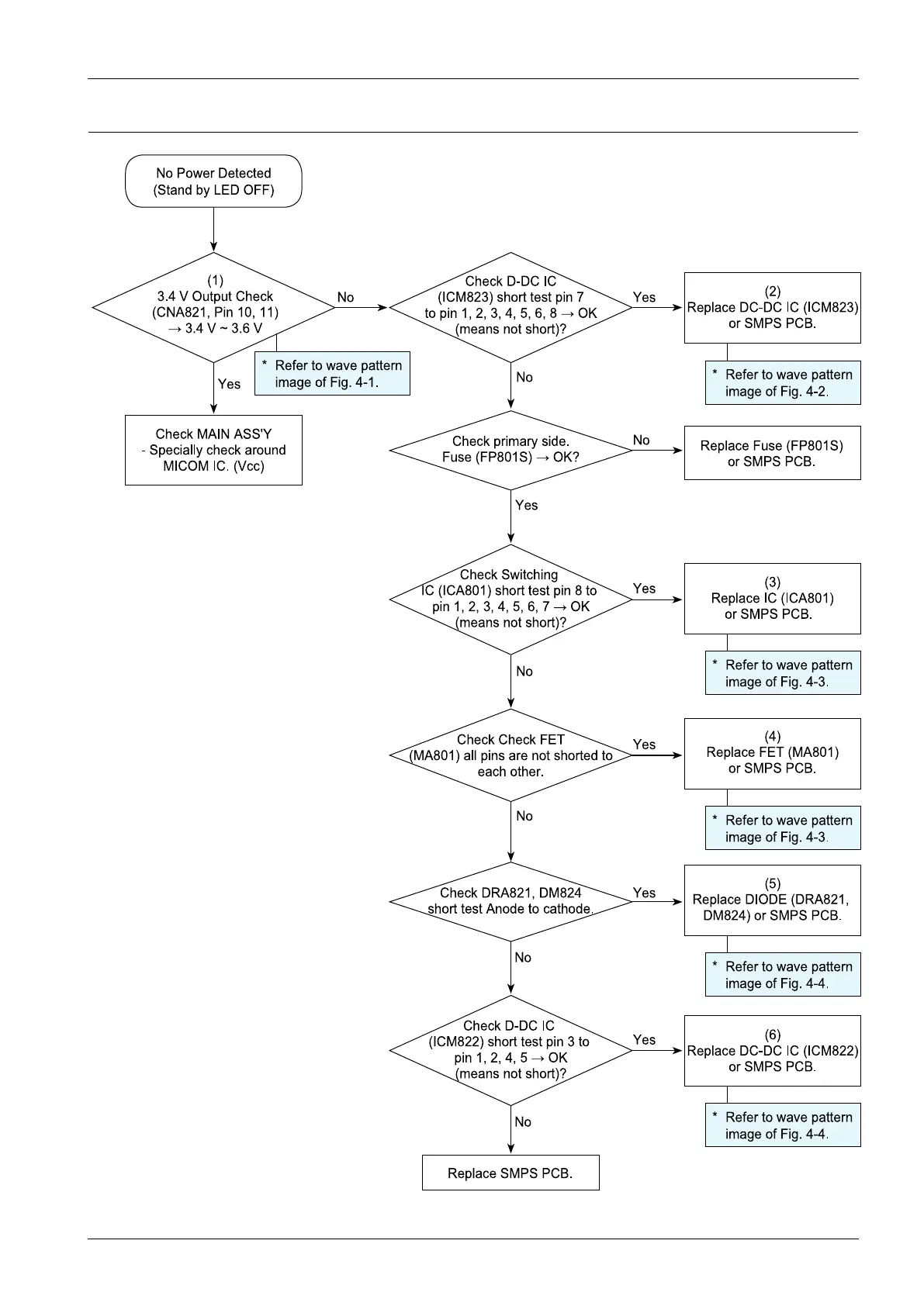
4.Troubleshooting
4.1.1.NoPower
Yes
Yes
Re place Fus e (FP801S )
or SMPS P CB.
Che ck MAIN AS S'Y
- Spe cially che ck a round
MICOM IC. (Vcc)
Che ck primary side .
Fuse (FP8 01S ) → OK?
Che ck D-DC IC
(ICM823) sh ort tes t pin 7
to p in 1, 2 , 3, 4 , 5, 6 , 8 → OK
(me a ns not sh ort)?
(1)
3.4 V Out put Che ck
(CNA821, P in 10, 11)
→ 3.4 V ~ 3 .6 V
(3)
Re place IC (ICA801)
or S MP S P CB.
(4)
Re place FET (MA801)
or SMPS P CB.
Che ck Che ck FE T
(MA801) a ll pins a re not shorte d to
ea ch othe r.
Che ck Sw itching
IC (ICA801) s hort te st p in 8 to
pin 1, 2, 3, 4, 5, 6, 7 → OK
(means not sh ort)?
YesNo
No
No
No
No
(5)
Re place DIODE (DRA821,
DM824) or S MP S P CB.
(2)
Re place DC-DC IC (ICM823)
or S MP S P CB.
(6)
Re place DC-DC IC (ICM822)
or S MP S P CB.
Re place S MP S P CB.
No
No
Yes
Yes
Yes
Yes
Che ck D-DC IC
(ICM822) short tes t pin 3 to
pin 1, 2, 4, 5 → OK
(means not sh ort)?
Che ck DRA821, DM824
short test Anode to ca thode .
No P owe r De tecte d
(Stand by LED OFF)
* Re fe r to wa ve pa tter n
image of Fig. 4-1 .
* Re fe r to wa ve pa tter n
image of Fig. 4-2.
* Re fe r to wa ve pa tter n
image of Fig. 4-3.
* Re fe r to wa ve pa tter n
image of Fig. 4-3.
* Re fe r to wa ve pa tter n
image of Fig. 4-4.
* Re fe r to wa ve pa tter n
image of Fig. 4-4.