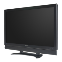
LC-52XS1E/RU/LC-65XS1E/RU
5 – 10
13.IC6702 (RH-iXC588WJN1Q)
This is a CPLD. By the SLOW BUS control, the extension I/O port for the reset signal and control signal sent to each device is created, and the
light control signal is generated.
14.IC6804 (VHiAK7770EQ-1Q)
This is an audio DSP, which implements the audio delay processing for the delay of the pictures of IC6201, the analog 2.1ch processing and the
SRS TruSurroundXT processing according to the I2S signal input from IC7103.
AUDIO-DSP
7 R/B# I READY BUSY
The Ready/Busy output is an Open Drain pin that signals the state of the memory.
12, 37 VCC - SUPPLY VOLTAGE
The VCC supplies the power for all the operations (Read, Write, Erase).
13,36 VSS - GROUND
1-6, 10-11, 14-15,
20-28, 33-35, 39-
40,45-48
NC - NO CONNECTION
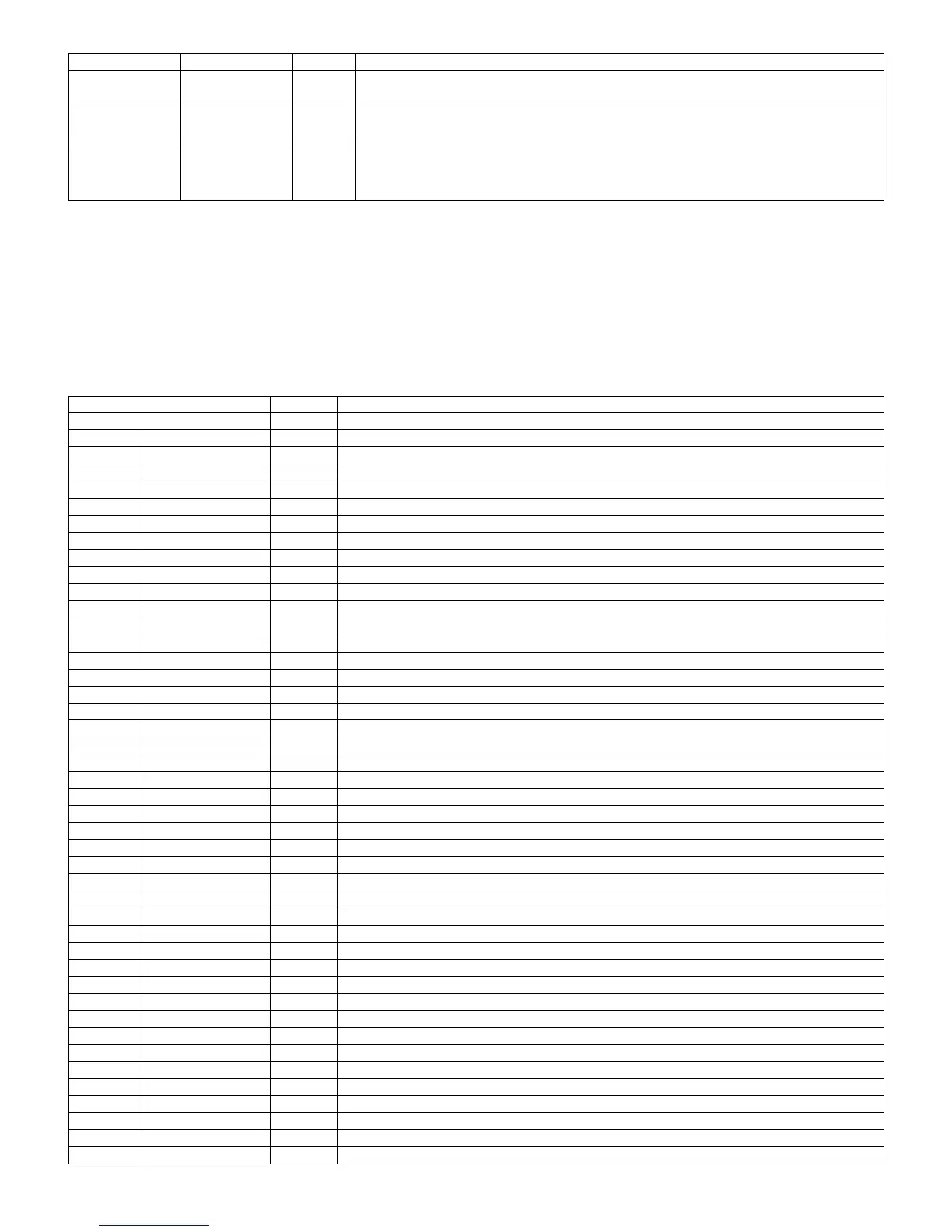
Pin No. Pin Name I/O Pin Function
1 FRIR1 I Rch feedback resistance input pin for ADC1
2 FRIL1 I Lch feedback resistance input pin for ADC1
3 FROL1 O Lch feedback resistance input pin for ADC1
4 LFLT - C connecting pin for PLL (10µF)
5 AVDD - Analog part power supply pin 3.3V
6 VSS1 - Analog part ground pin 0V
7 TESTI I Test pin (with pull down resistance)
8 CKM[0] I Clock mode select pin
9 HMUTEN I Headphone amplifier mute pin
10 INITRSTN I Initial reset pin (for initialization)
11 SETROM I The pin for ROM boot
12 DVDD18 - Digital part power supply pin 1.8V
13 VSS3 - Digital part grand pin 0V
14 DVDD18 - Digital part power supply pin 3.3V
15 LRCLKO O LR channel selection output pin
16 CLKO O Clock output pin
17 BITCLKO O Serial bit clock output pin
18 SDOUT1 O Serial-data output 1 pin
19 SDOUT2 O Serial-data output 2 pin
20 SDOUT3 O Serial-data output 3 pin
21 XTO O Oscillating circuit output pin
22 XTI I Oscillating circuit input pin
23 DVDD - Digital part power supply pin 3.3V
24 VSS3 - Digital part ground pin 0V
25 DVDD18 - Digital part power supply pin 1.8V
26 LRCLK1 I LR channel selection input pin
27 CLK1 I Serial master clock 1 pin
28 BITCLK1 I Serial bit clock 1 pin
29 SDIN1 I Serial-data input 1 pin
30 LRCLK2 I LR channel selection input 2 pin
31 CLK2 I Serial master clock 2 pin
32 BITCLK2 I Serial bit clock 2 pin
33 SDIN2 I Serial-data input 2 pin
34 CAD1 I I2 C-bus address 1 pin
35 CAD0 I I2 C-bus address 0 pin
36 SCL I SCL I2C Clock pin
37 DVDD - Digital part power supply pin 3.3V
38 VSS3 - Digital part ground pin 0V
39 DVDD18 - Digital part power supply pin 1.8V
40 SDA I/O SDA I2C Bus interface
41 HPEN O The pin for headphone detection
42 STO O Status output pin
43 TX O S/PDIF Transmitter output pin
44 DVDD - Digital part power supply pin 3.3V
Pin No. Pin Name I/O Pin Function
 Loading...