7SR224 Argus Description of Operation
List of Figures
Figure 1.5-1 Functional Diagram of 7SR224 Relay Showing Possible External Connections ...........8
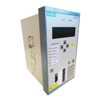
Figure 2.5-1 7SR224 with 12 Function Keys and 3 + 8 LEDs in E10 Case......................................10
Figure 2.8-1 Binary Input Logic .........................................................................................................13
Figure 2.9-1 Binary Output Logic ......................................................................................................15
Figure 3.1-1 Logic Diagram: Directional Overcurrent Element (67)..................................................18
Figure 3.1-2 Logic Diagram: Instantaneous Over-current Element ..................................................19
Figure 3.1-3 Logic Diagram: Time Delayed Overcurrent Element....................................................21
Figure 3.2-1 Logic Diagram: Voltage Controlled Overcurrent Protection .........................................22
Figure 3.3-1 Logic Diagram: Measured Directional Earth Fault Protection ......................................24
Figure 3.3-2 Logic Diagram: Measured Instantaneous Earth-fault Element.....................................24
Figure 3.3-3 Logic Diagram: Measured Time Delayed Earth Fault Element (51G)..........................25
Figure 3.4-1 Logic Diagram: SEF Directional Element (67SEF).......................................................26
Figure 3.4-2 Logic Diagram: SEF Instantaneous Element ...............................................................27
Figure 3.4-3 Logic Diagram: SEF Time Delayed Element (51SEF) .................................................28
Figure 3.5-1 Logic Diagram: High Impedance REF (64H)................................................................29
Figure 3.6-1 Logic Diagram: Cold Load Settings (51c).....................................................................30
Figure 3.7-1 Logic Diagram: Negative Phase Sequence Overcurrent (46NPS)...............................31
Figure 3.8-1 Logic Diagram: Undercurrent Detector (37) .................................................................32
Figure 3.9-1 Logic Diagram: Thermal Overload Protection (49S) ....................................................34
Figure 3.10-1 Logic Diagram: Under/Over Voltage Elements (27/59)................................................35
Figure 3.11-1 Logic Diagram: NPS Overvoltage Protection (47)........................................................36
Figure 3.12-1 Logic Diagram: Neutral Overvoltage Element ..............................................................37
Figure 3.13-1 Logic Diagram: Under/Over Frequency Detector (81)..................................................38
Figure 4.1-1 Typical Autoreclose Sequence with 3 Instantaneous and 1 Delayed trip ....................41
Figure 4.1-2 Basic Autoreclose Sequence Diagram .........................................................................46
Figure 4.3-1 Voltage Detector Operation ..........................................................................................48
Figure 4.3-2 Check Sync Function....................................................................................................49
Figure 4.3-3 System Sync Function ..................................................................................................51
Figure 4.3-4 Cloze On Zero Function................................................................................................51
Figure 4.4-1 Logic Diagram: Circuit Breaker Status .........................................................................53
Figure 4.5-1 Sequence Diagram: Quick Logic PU/DO Timers (Counter Reset Mode Off)...............55
Figure 5.1-1 Logic Diagram: Circuit Breaker Fail Protection (50BF) ................................................56
Figure 5.2-1 Logic Diagram: VT Supervision Function (60VTS).......................................................58
Figure 5.3-1 Logic Diagram: CT Supervision Function (60CTS) ......................................................59
Figure 5.4-1 Logic Diagram: Broken Conductor Function (46BC) ....................................................60
Figure 5.5-1 Logic Diagram: Trip Circuit Supervision Feature (74TCS)...........................................60
Figure 5.6-1 Logic Diagram: Harmonic Block Feature (81HBL2) .....................................................61
Figure 5.7-1 Battery Test timing diagram..........................................................................................62
Figure 5.8-1 Capacitor Test timing diagram......................................................................................63
Figure 5.9-1 Sag and Swell Indices - IEEE 1159..............................................................................64
List of Tables
Table 1-1 7SR224 Ordering Options ..............................................................................................7
Table 2-1 Summary of Controller Relay Configurations .................................................................9
Table 6-1 Operation Mode ............................................................................................................68
©2010 Siemens Protection Devices Limited Chapter 1 Page 4 of 70
 Loading...