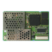
MC45 Hardware Interface Description
P R E L I M I N A R Y
MC45_HD_01_V00.02a Page 25 of 90 12.08.2002
3.2 Power supply
The power supply of MC45 has to be a single voltage source of V
BATT+
= 3.3V...4.5V. It must
be able to provide sufficient current in a transmit burst which typically rises to 2A. Beyond
that, the power supply must be able to account for increased current consumption if the
module is exposed to inappropriate conditions, for example antenna mismatch. For further
details see Chapters 3.2.2 and 6.4.1.
All the key functions for supplying power to the device are handled by an ASIC power
supply. The ASIC provides the following features:
· Stabilizes the supply voltages for the GSM baseband using low drop linear voltage
regulators.
· Controls the module's power up and s procedures.
A watchdog logic implemented in the baseband processor periodically sends signals to
the ASIC, allowing it to maintain the supply voltage for all digital MC45 components.
Whenever the watchdog pulses fail to arrive constantly, the module is turned off.
· Delivers, across the VDD pin, a regulated voltage of 2.9V. The output voltage VDD may
be used to supply, for example, an external LED or a level shifter. However, the external
circuitry must not cause any spikes or glitches on voltage VDD. This voltage is not
available in POWER DOWN mode. Therefore, the VDD pin can be used to indicate
whether or not MC45 is in POWER DOWN mode.
· Includes a switch to provide power to the SIM interface.
The RF power amplifier is driven directly from BATT+.
3.2.1 Power supply pins on the board-to-board connector
Five BATT+ pins of the board-to-board connector are dedicated to connect the supply
voltage, five GND pins are recommended for grounding. The POWER and CHARGE pins
serve as control signals for charging a Li-Ion battery. VDDLP can be used to back up the
RTC.
Table 4: Power supply pins of board-to-board connector
Signal name I/O Description Parameter
BATT+ I/O Positive operating voltage
3.3 V...4.5 V, I
typ
£ 2 A during transmit burst
The minimum operating voltage must not fall
below 3.3 V, not even in case of voltage drop.
GND - Ground 0 V
POWER I This line signalizes to the
processor that the charger
is connected.
CHARGE O Control signal for external
charging transistor
VDDLP I/O Can be used to back up the
RTC when V
BATT+
is not
applied.
See Chapter 3.4
U
OUT,max
< V
BATT+
U
IN
= 2.0 V...5.5 V
R
i
= 1kW
I
in,max
= 30µA